Optical module and method of packaging the same

a technology of optical modules and optical modules, applied in multiplex communication, semiconductor lasers, instruments, etc., can solve the problems of increasing cost and time for manufacturing the module, not allowing passive alignment to be applied to the structure of the optical module, etc., to achieve simple and low-cost configuration, simple and low-cost

Inactive Publication Date: 2009-12-29
NEC CORP
View PDF18 Cites 4 Cited by
  • Summary
  • Abstract
  • Description
  • Claims
  • Application Information

AI Technical Summary

Benefits of technology

[0011]Aspects of the present invention provide an optical module and a method of packaging the optical module, which enables long-distance and large-volume communications by using a simple configuration.
[0018]According to exemplary embodiments of the present invention, it is possible to realize an optical module in a simple and low-cost configuration by packaging the single-mode oscillating light source and the optical filter by passive alignment without active alignment. Further, by using an optical filter such as a waveguide ring resonator, which converts a frequency modulation to an amplitude modulation, it is possible to realize an optical module in a simple and low-cost configuration. This is because the waveguide ring resonator is much cheaper and smaller than generally used expensive and bulky modulators such as a LiNbO3 (LN) modulator. Further, by using an optical filter such as the waveguide ring resonator, optical signals whose wavelength chirping is low can be obtained. And, these characteristics are suitable for long-distance and large-volume optical communication.

Problems solved by technology

This does not allow passive alignment to be applied to the structure of the optical module.
Without such passive alignment, the cost and the time for manufacturing the module will increase.
And, this does not allow passive alignment to be applied to the structure of the optical module.
However, this optical module is too large to meet the requirement of miniaturization of the module.

Method used


Image

  • Optical module and method of packaging the same
  • Optical module and method of packaging the same
  • Optical module and method of packaging the same

Examples


Embodiment Construction

[0029]Exemplary embodiments of the invention will now be described below with reference to the attached Figures. The described exemplary embodiments are intended to assist the understanding of the invention, and are not intended to limit the scope of the invention in any way.

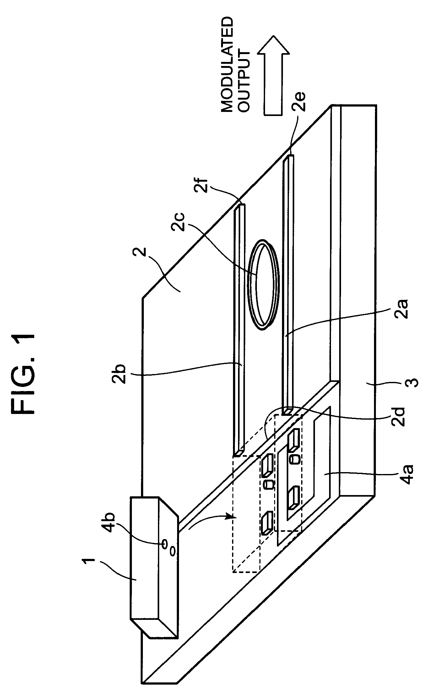
[0030]FIG. 1 is a perspective view showing an optical module according to an exemplary embodiment of the present invention.

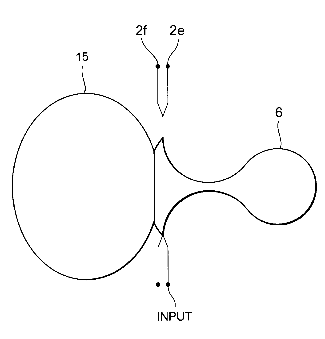
[0031]FIG. 1 shows that a DFB laser 1 capable of a high-speed modulation which is used as a single-mode oscillating light source, and a waveguide ring resonator 2 which is used as an optical filter are packaged without active alignment on the same substrate 3.

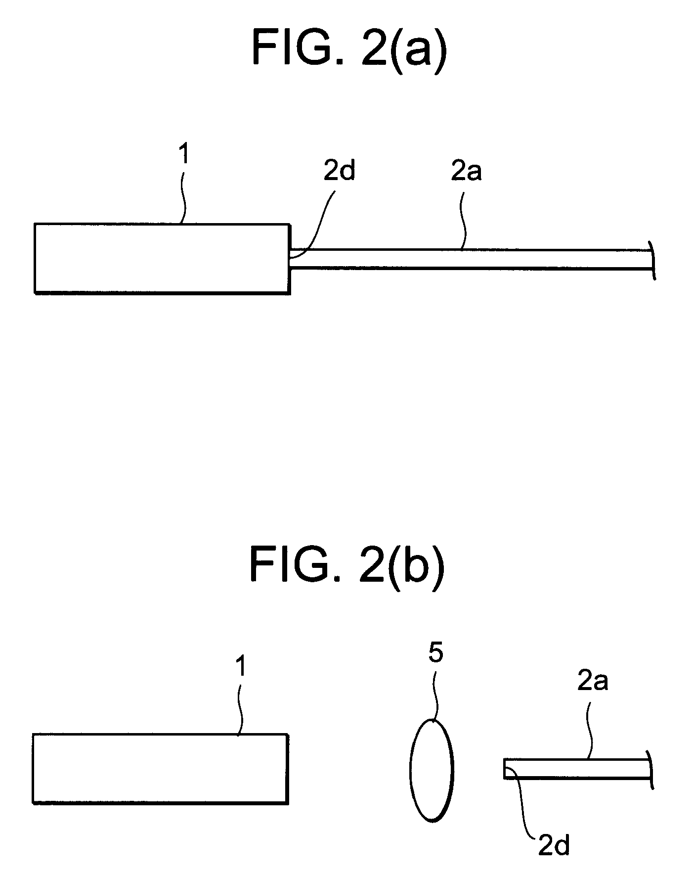
[0032]That is, the DFB laser 1 and the waveguide ring resonator 2 are packaged by passive alignment on the same substrate 3 (the package of this type is also termed as a “flip-chip package”). The passive alignment technique is carried out as follows. First, alignment markers 4a and 4b are provided on the substrate 3 and the DFB laser 1,...


PUM

PropertyMeasurementUnit
transmission distanceaaaaaaaaaa
frequencyaaaaaaaaaa
lengthsaaaaaaaaaa

Abstract

An optical module is configured with a combination of a single-mode oscillating light source and an optical filter. In this optical module, the single-mode oscillating light source outputs a single-mode, frequency-modulated signal. Further, the optical filter converts the frequency modulation to an amplitude modulation. And, the single-mode oscillating light source and the optical filter are packaged without active alignment on the same substrate. Accordingly, it is possible to realize an optical module in a simple and low-cost configuration by packaging the single-mode oscillating light source and the optical filter by passive alignment, without active alignment, on the same substrate, and by using a simple optical filter such as a waveguide ring resonator, which converts a frequency modulation to an amplitude modulation.

Description

CROSS-REFERENCE TO RELATED APPLICATION[0001]This application claims priority from Japanese Patent Application No. 2006-170388, filed on Jun. 20, 2006, in the Japanese Patent Office, the disclosure of which is hereby incorporated by reference in its entirety.BACKGROUND[0002]1. Field[0003]Apparatuses and manufacturing methods consistent with the present invention relate to an optical module for a high-speed and large-volume optical communications system, and to a method of packaging the same.[0004]2. Description of the Related Art[0005]Along with the spread of the Internet, the development of a high-speed and large-volume optical communication system has been achieved. Especially in a long-distance and large-volume communications system, efforts have been made to reduce wavelength fluctuation (hereinafter referred to as “wavelength chirping”), which occurs during modulation, because such wavelength chirping limits the transmission distance. A frequency pulse laser (FP laser) of end-su...

Claims


Application Information

Patent Timeline
Patent Type & Authority Patents(United States)
IPC IPC(8): G02B6/26G02B6/32G02F1/01G02F1/00G02B6/12G02B6/00G02B6/28G02F1/295H04J14/02H04J14/00G02F1/23G02F1/09H01S3/08H01S3/10H01S3/13G02F1/11G02B6/122H01S5/022H01S5/50
CPCG02B6/4224G02B6/4204G02B6/12G02B6/293
Inventor YAMAZAKI, HIROYUKIHATANAKA, TAKAAKI
Owner NEC CORP
Why Eureka
Try Eureka