Semiconductor memory device having local etch stopper and method of manufacturing the same
- Summary
- Abstract
- Description
- Claims
- Application Information
AI Technical Summary
Problems solved by technology
Method used
Image

Examples
Embodiment Construction
[0026] Exemplary embodiments of the invention are described below with reference to the corresponding drawings. These embodiments are presented as teaching examples. The actual scope of the invention is defined by the claims that follow.
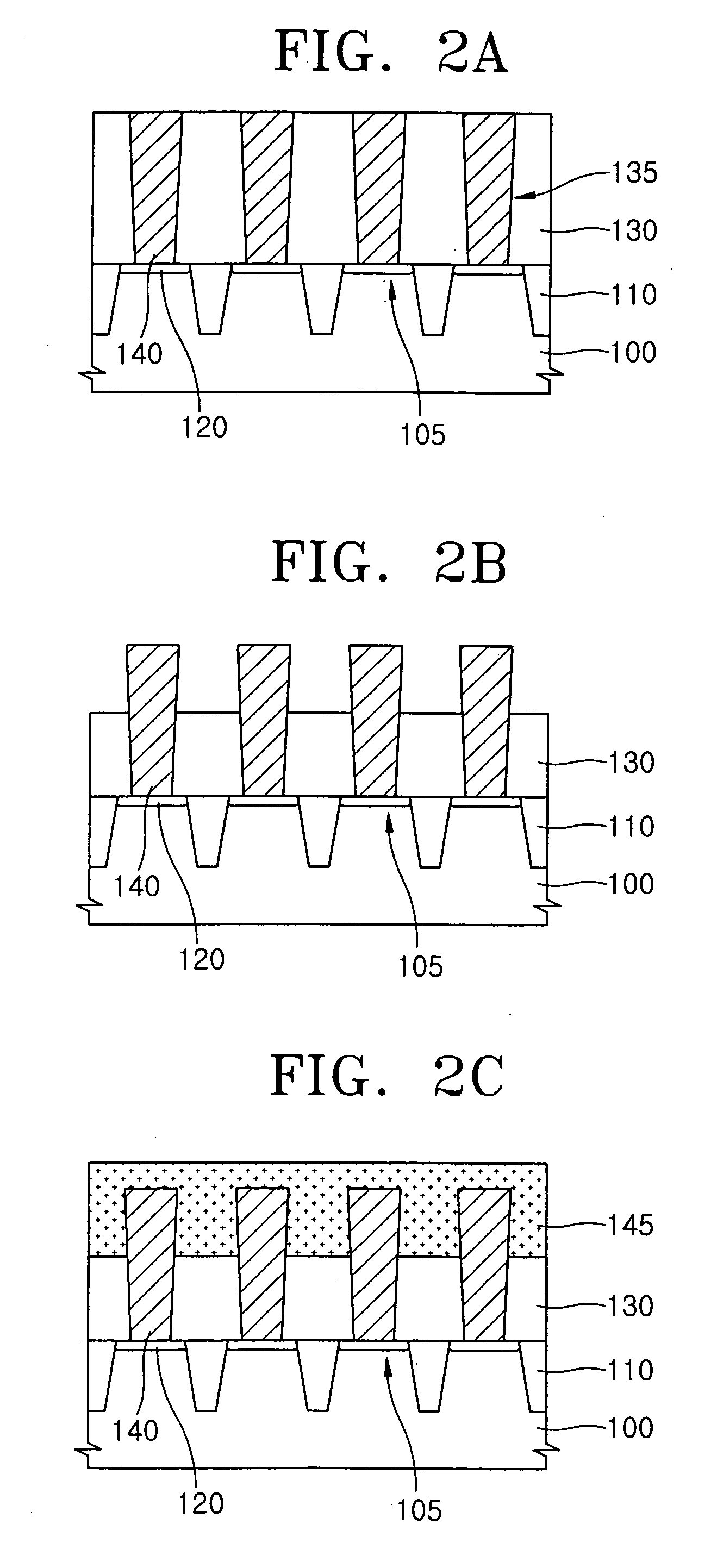
[0027]FIGS. 2A through 2E are cross-sectional views illustrating a method of manufacturing a semiconductor memory device according to an embodiment of the present invention.
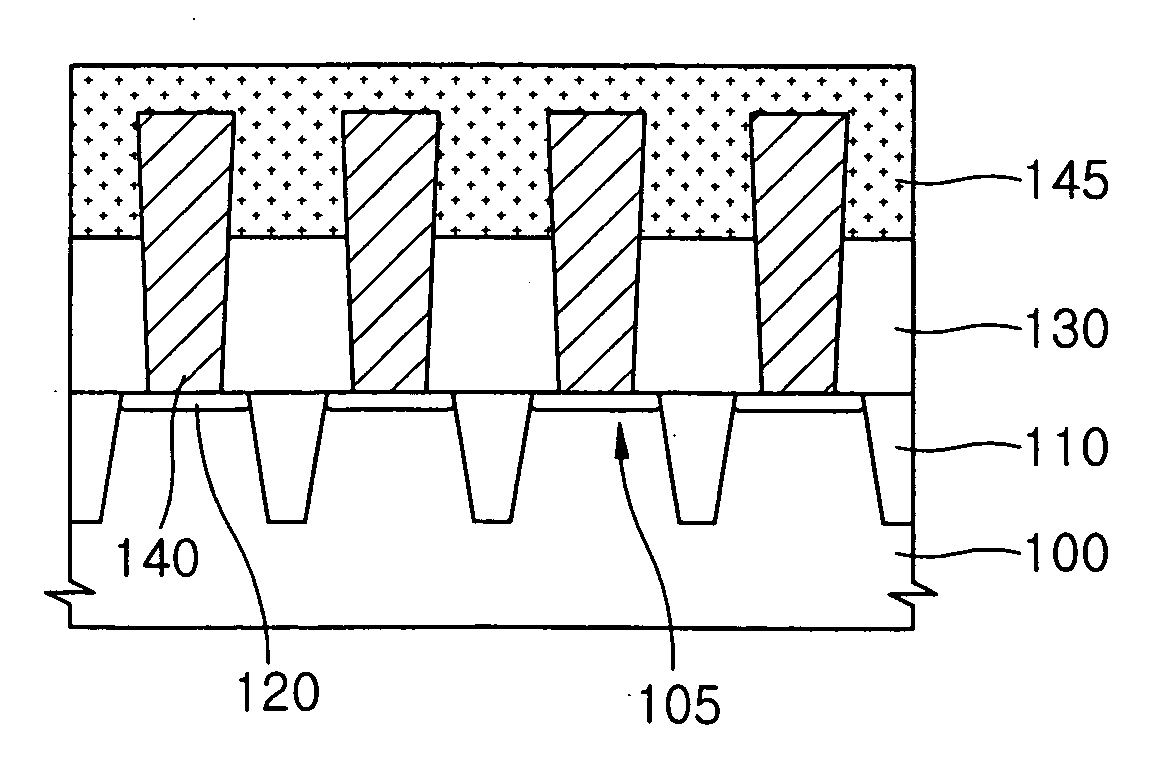
[0028] Referring to FIG. 2A, isolation layers 110 are formed in predetermined portions of a semiconductor substrate 100 to define active regions 105. Isolation layers 110 are typically formed by shallow trench isolation (STI). A conductive region 120 is formed in each active region 105 between isolation layers 110. Conductive regions 120 are typically formed by implanting impurities in semiconductor substrate 100. A first insulating interlayer 130 comprising silicon oxide is formed on semiconductor substrate 100. First insulating interlayer 130 is then etched to form contact hol...
PUM
 Abstract
Description
Claims
Application Information
PatSnap Eureka turns technology decisions into work you can execute. Powered by our Innovation Knowledge Graph, it runs expert workflows across engineering, life sciences, materials and intellectual property. Get your review-ready output in minutes.


