Oled device having improved light output

a light-emitting diode and light-emitting layer technology, which is applied in the direction of discharge tube luminescnet screens, discharge tube/lamp details, electric discharge lamps, etc., can solve the problems of limiting the efficiency of oled devices, affecting the sharpness of the light-emitting layer, and absorbing a large amount of light within the device. , to achieve the effect of improving the sharpness, increasing the light output and improving the sharpness

Active Publication Date: 2006-08-24
GLOBAL OLED TECH
View PDF24 Cites 154 Cited by
  • Summary
  • Abstract
  • Description
  • Claims
  • Application Information

AI Technical Summary

Benefits of technology

[0017] The present invention:has the advantage that it increases the light output from, and improves the sharpness of, an OLED device.

Problems solved by technology

However, as is well known, much of the light output from the light-emissive layer in the OLED is absorbed within the device.
In general, up to 80% of the light may be lost in this manner.
It has been found, however, that one of the key factors that limits the efficiency of OLED devices is the inefficiency in extracting the photons generated by the electron-hole recombination out of the OLED devices.
Due to the high optical indices of the organic materials used, most of the photons generated by the recombination process are actually trapped in the devices due to total internal reflection.
However, none of these approaches cause all, or nearly all, of the light produced to be emitted from the device.
Moreover, such diffractive techniques cause a significant frequency dependence on the angle of emission so that the color of the light emitted from the device changes with the viewer's perspective.
However, considerable light is still lost through absorption of the light as it travels laterally through the layers parallel to the substrate within a single pixel or light emitting area.
However, scattering techniques, by themselves, cause light to pass through the light-absorbing material layers multiple times where they are absorbed and converted to heat.
Moreover, trapped light may propagate a considerable distance horizontally through the cover, substrate, or organic layers before being scattered out of the device, thereby reducing the sharpness of the device in pixellated applications such as displays.
Moreover, if applied to display devices, this structure will decrease the perceived sharpness of the display.
The particular arrangements, however, may still result in reduced sharpness of the device.

Method used


Image

  • Oled device having improved light output
  • Oled device having improved light output
  • Oled device having improved light output

Examples


Embodiment Construction

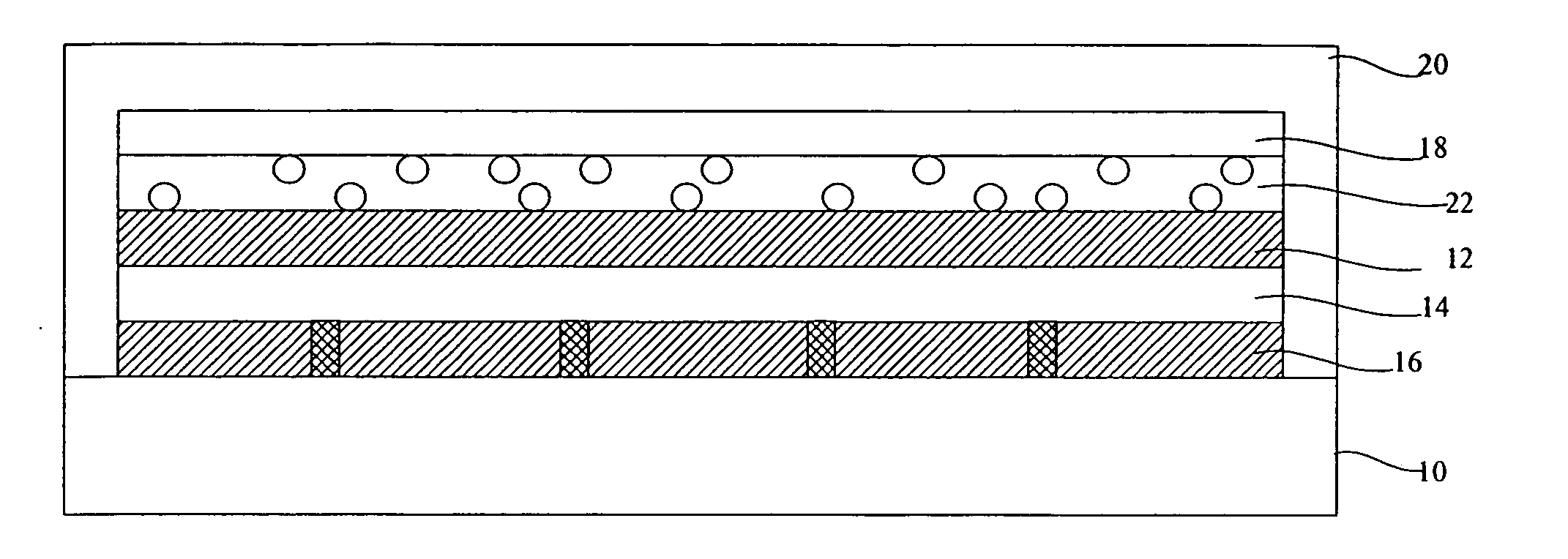
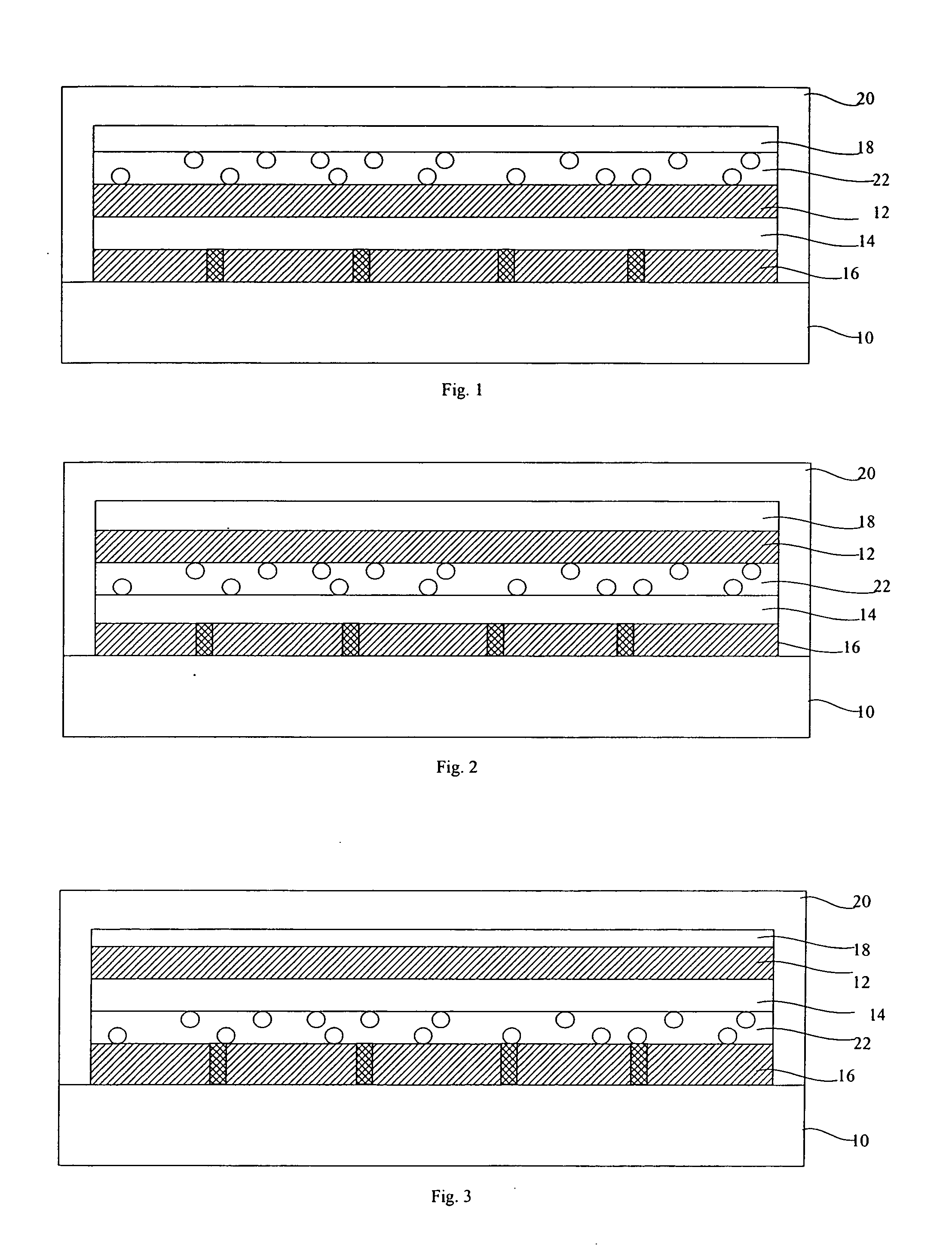
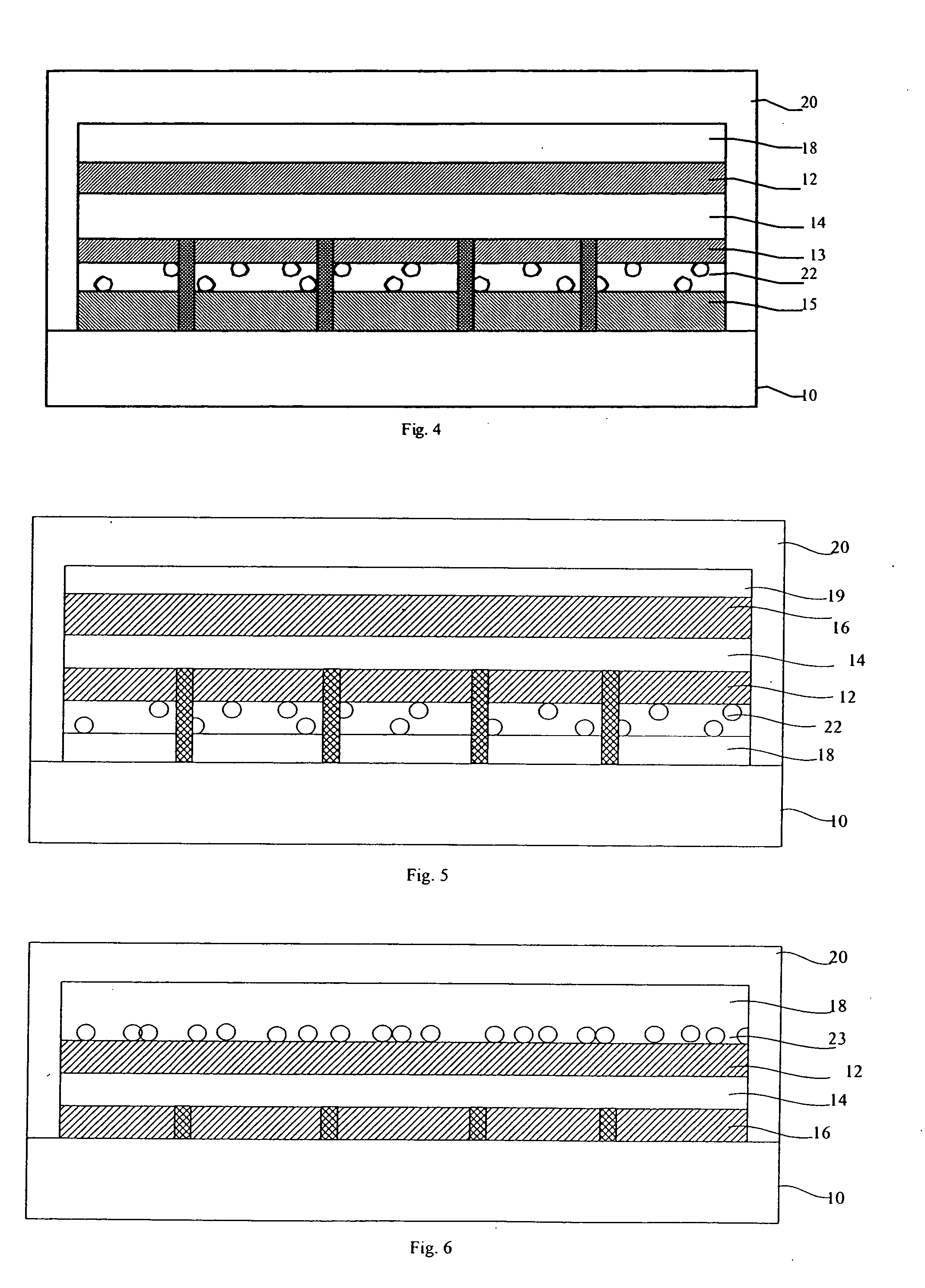
[0036] Referring to FIG. 1, in accordance with one embodiment, a top-emitting organic light-emitting diode. (OLED) device comprises a substrate 10; an OLED comprising a first reflective electrode 16 and a second transparent electrode 12, one or more layers 14 of organic light-emitting material formed between the electrodes 12 and 16, and an encapsulating transparent cover 20 through which light from the OLED is emitted. Either one of the first or second electrodes 12 or 16 may be pixellated to form distinct light emitting areas. The transparent electrode 12 and layer(s) 14 of organic light-emitting material have a first refractive index range, and the transparent cover 20 has a second refractive index. A light scattering layer 22 is located between the substrate and cover, in this embodiment between the transparent electrode 12 and the cover 20. As employed herein, a light scattering layer is an optical layer that tends to randomly redirect any light that impinges on the layer from ...


PUM


Abstract

An organic light-emitting diode (OLED) device, comprising: a substrate; an OLED comprising first and second electrodes and one or more layers of organic light-emitting material formed between the electrodes, wherein at least one electrode comprises a transparent electrode, the transparent electrode and layer(s) of organic light-emitting material having a first refractive index range; and an encapsulating cover; wherein at least one of the substrate or cover comprises a transparent substrate or cover having a second refractive index and through which light from the OLED is emitted; and further comprising a light scattering layer located between the substrate and cover, and a transparent low-index element having a third refractive index lower than each of the first refractive index range and second refractive index and located between the scattering layer and the transparent substrate or cover.

Description

FIELD OF THE INVENTION [0001] The present invention relates to organic light-emitting diode (OLED) devices, and more particularly, to OLED device structures for improving light output. BACKGROUND OF THE INVENTION [0002] Organic light-emitting diodes (OLEDs) are a promising technology for flat-panel displays and area illumination lamps. The technology relies upon thin-film layers of materials coated upon a substrate. However, as is well known, much of the light output from the light-emissive layer in the OLED is absorbed within the device. Because light is emitted in all directions from the internal layers of the OLED, some of the light is emitted directly from the device, and some is emitted into the device and is either reflected back out or is absorbed, and some of the light is emitted laterally and trapped and absorbed by the various layers comprising the device. In general, up to 80% of the light may be lost in this manner. [0003] OLED devices generally can have two formats know...

Claims


Application Information

Patent Timeline
Patent Type & Authority Applications(United States)
IPC IPC(8): H05B33/04
CPCH01L51/5203H01L51/5237H01L51/5268H01L51/5275H10K50/805H10K50/841H10K50/854H10K50/858
Inventor COK, RONALD S.PREUSS, DONALD R.TYAN, YUAN-SHENG
Owner GLOBAL OLED TECH
Why Eureka
Try Eureka