High density interconnect system for IC packages and interconnect assemblies

Inactive Publication Date: 2006-08-24
ADVANTEST SINGAPORE PTE LTD
View PDF99 Cites 96 Cited by
  • Summary
  • Abstract
  • Description
  • Claims
  • Application Information

AI Technical Summary

Benefits of technology

[0027] An improved interconnection system and method is described, such as for electrical contactors and connectors, electronic device or module package assemblies, socket assemblies and/or probe card assembly systems. An exemplary interconnection system comprises a first connector structure comprising a contactor substrate having a contactor surface and a bonding surface, and a set of at least one electrically conductive micro-fabricated spring contact extending from the contact surface, a second connector structure having a set of at least one electrically conductive contact pad located on a connector su

Problems solved by technology

Nonetheless, the size of portable electronic systems such as portable computers, cell phones, PDAs, etc. continues to shrink despite the addition of new features and functions.
However, over time, the size of most portable electronics systems tends to decrease.
Less space is available for power sources and heat dissipation structures.
Despite increases in the number and density of input/output (I/O) pads on each die, the footprint and thickness of electronic systems continues to shrink since the individual components and/or devices integrated into these systems tend to decrease with each successive tec

Method used


Image

  • High density interconnect system for IC packages and interconnect assemblies
  • High density interconnect system for IC packages and interconnect assemblies
  • High density interconnect system for IC packages and interconnect assemblies

Examples


Embodiment Construction

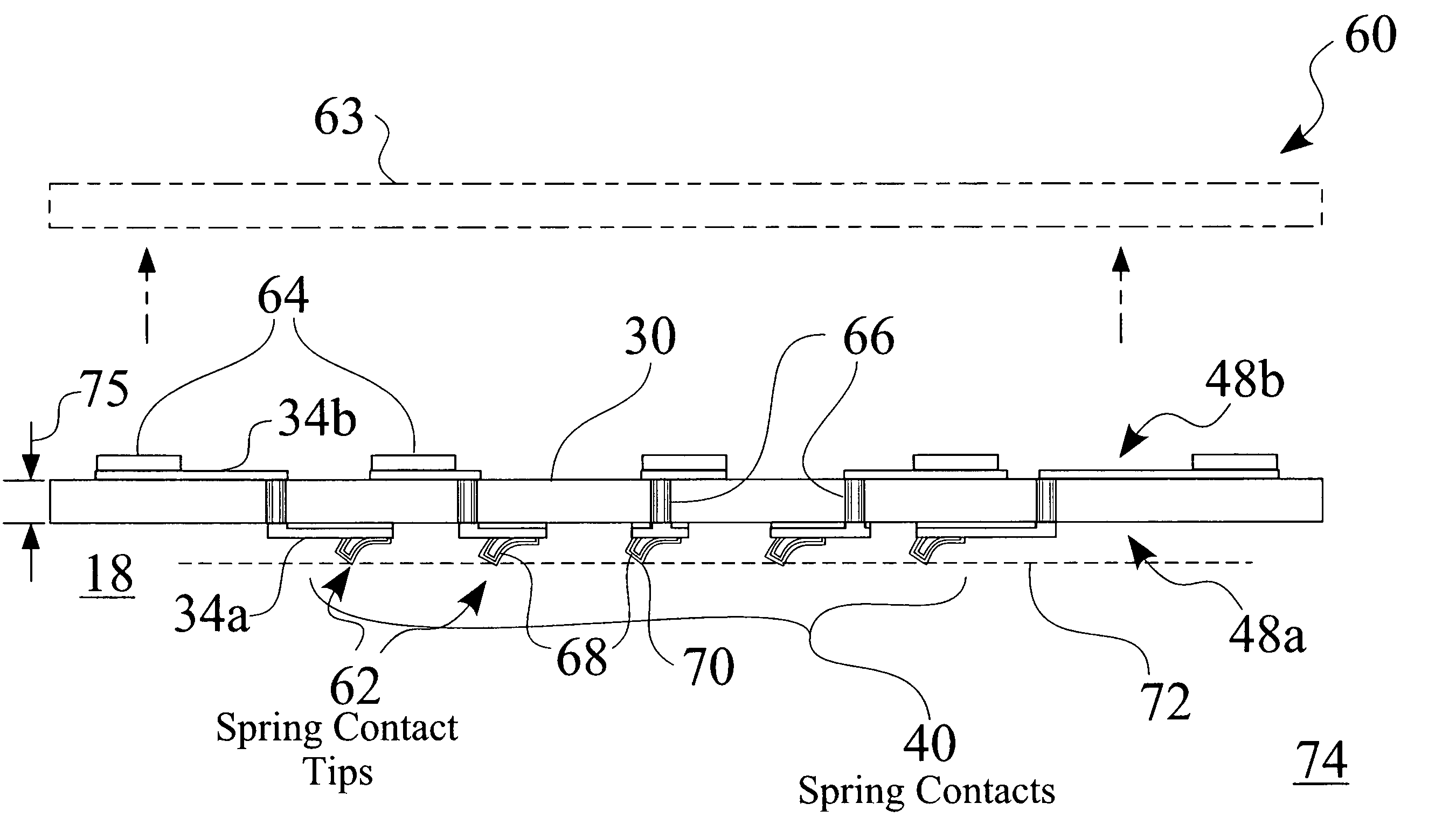
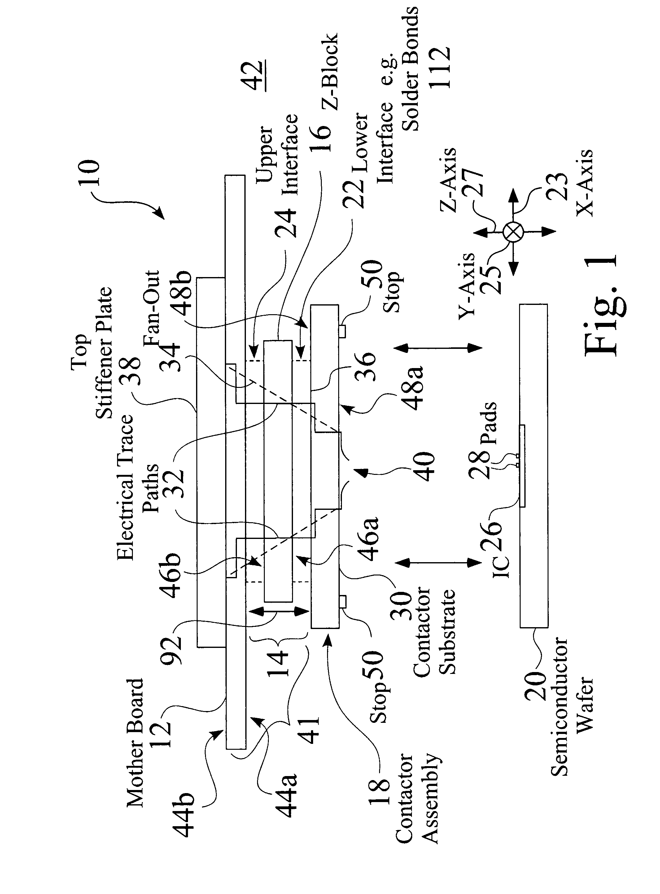
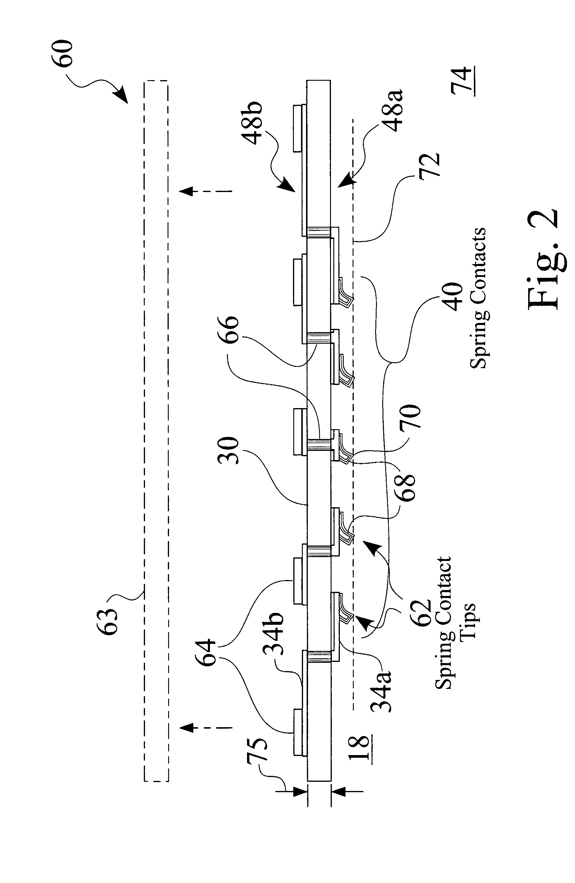
[0067] Introductory disclosure regarding structures, processes and systems disclosed herein is seen in: U.S. Provisional Application No. 60 / 136,636, entitled Wafer Interface for High Density Probe Card, filed 27 May 1999; U.S. Provisional Application No. 60 / 146,241, entitled Method of Massively Parallel Testing of Circuits, filed 28 Jul. 1999; U.S. Provisional Application No. 60 / 573,541, entitled Quick-Change Probe Chip, filed 20 May 2004; U.S. Provisional Application No. 60 / 592,908, entitled Probe Card Assembly with Rapid Fabrication Cycle, filed 29 Jul. 2004; U.S. Provisional Application No. 60 / 651,294, entitled Nano-Contactor Embodiments for IC Packages and Interconnect Components, filed 8 Feb. 2005; U.S. patent application Ser. No. 10 / 870,095, entitled Enhanced Compliant Probe Card Systems Having Improved Planarity, US Filing Date 16 Jun. 2004; U.S. patent application Ser. No. 10 / 178,103, entitled Construction Structures and Manufacturing Processes for Probe Card Assemblies and ...


PUM


Abstract

An improved interconnection system is described, such as for electrical contactors and connectors, electronic device or module package assemblies, socket assemblies, and/or probe card assembly systems. An exemplary connector comprises a first connector structure comprising a contactor substrate having a contact surface and a bonding surface, and one or more electrically conductive micro-fabricated spring contacts extending from the probe surface, a second connector structure comprising at least one substrate and having a set of at least one electrically conductive contact pad located on a connector surface and corresponding to the set of spring contacts, and means for movably positioning and aligning the first connector structure and the second connector structure between at least a first position and a second position, such that in at least one position, at least one electrically conductive micro-fabricated spring contact is electrically connected to at least one electrically conductive contact pad.

Description

CROSS REFERENCE TO RELATED APPLICATIONS [0001] This Application claims priority to U.S. Provisional Application No. 60 / 651,294, entitled Nano-Contactor Embodiments for IC Packages and Interconnect Components, filed 8 Feb. 2005, and to U.S. Provisional Application No. 60 / 718,137, entitled Compliant Nanocontactors for Application in Portable and High Density Electronic Systems, filed 16 Sep. 2005, each of which are incorporated herein in its entirety by this reference thereto. [0002] This Application is also a Continuation In Part of U.S. patent application Ser. No. 11 / 133,021, entitled High Density Interconnect System Having Rapid Fabrication Cycle, US Filing Date 18 May 2005, which is a Continuation In Part of U.S. patent application Ser. No. 10 / 870,095, entitled Enhanced Compliant Probe Card Systems Having Improved Planarity, US Filing Date 16 Jun. 2004, which is a Continuation In Part of U.S. patent application Ser. No. 10 / 178,103, entitled Construction Structures and Manufacturin...

Claims


Application Information

Patent Timeline
IPC IPC(8): G01R31/02
CPCG01R1/0483G01R1/07342G01R1/06716G01R3/00G01R1/07378
Inventor BOTTOMS, W. R.CHONG, FU CHIUNGMOK, SAMMYMODLIN, DOUGLAS
Owner ADVANTEST SINGAPORE PTE LTD
Why Eureka
Try Eureka