
Light emitting element driving circuit, and optical transmission apparatus and optical transmission system using the same

a technology of driving circuit and light emitting element, which is applied in the direction of electrical equipment, semiconductor lasers, laser details, etc., can solve the problems of device disassembly, 78 mw, and deviation from the safety standard

Inactive Publication Date: 2006-08-24
FUJIFILM BUSINESS INNOVATION CORP
View PDF7 Cites 12 Cited by
  • Summary
  • Abstract
  • Description
  • Claims
  • Application Information

AI Technical Summary

Benefits of technology

[0018] Therefore, it is an object of the invention to provide a light emitting element driving circuit in which, even when an AC-coupling capacitor for superposing a modulating current to a bias current is short-circuited, abnormal light emission is prevented from occurring in a light emitting element, and peripheral devices can be protected, and also an optical transmission apparatus, a laser printer, and a laser writing apparatus which use the light emitting element driving circuit.
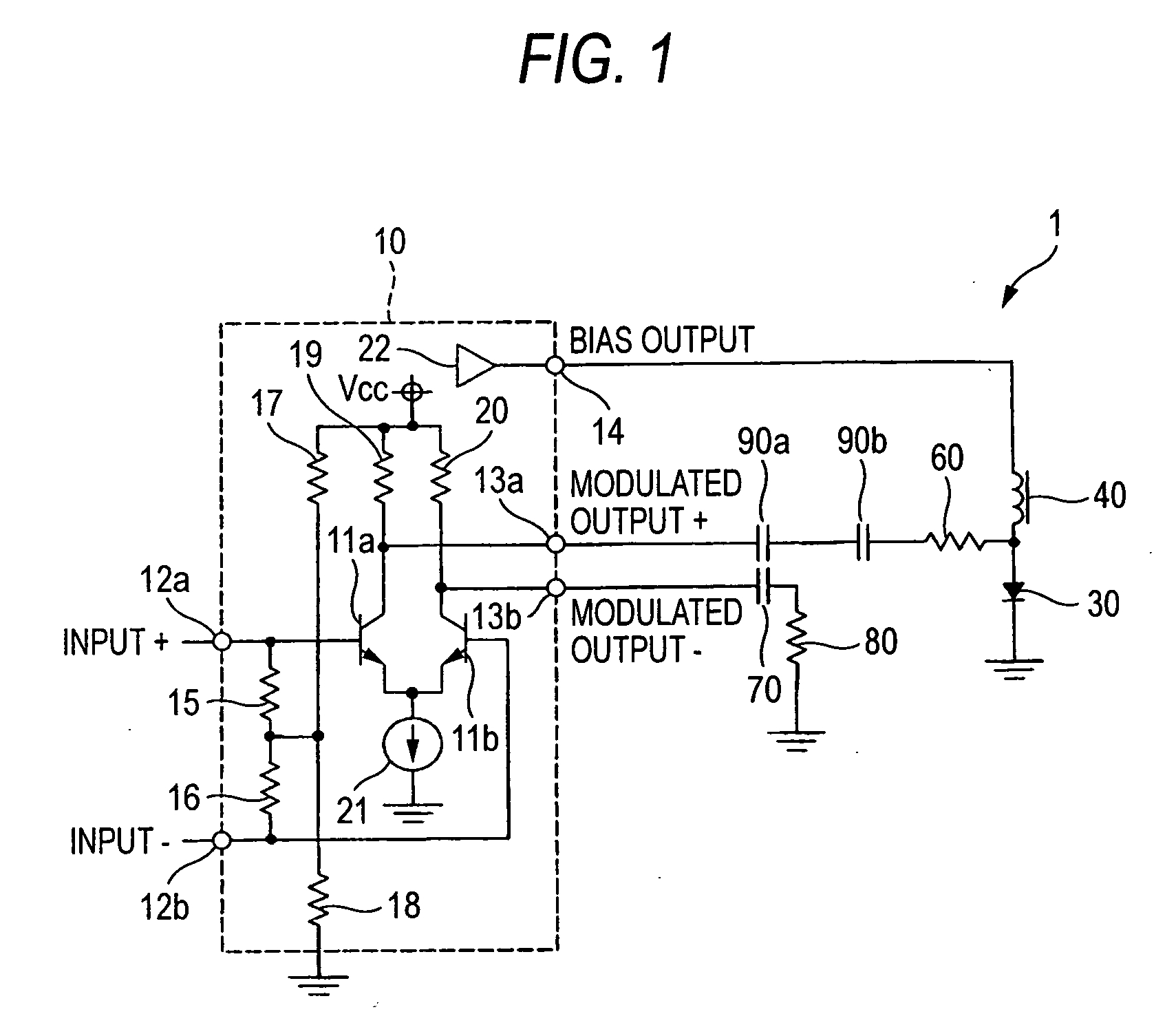
[0023] The plural AC-coupling capacitors may be connected between an output terminal for the modulating current and the anode of the semiconductor laser. According to the configuration, even when one of the plural AC-coupling capacitors breaks to enter a short-circuit state, the AC coupling is maintained by the other AC-coupling capacitor(s). Therefore, an excessive current can be prevented from flowing through the semiconductor laser.
[0030] According to the invention, even when an AC-coupling capacitor for superposing a modulating current to a bias current is short-circuited, abnormal light emission is prevented from occurring in the light emitting element, and peripheral devices can be protected.

Problems solved by technology

Consequently, there is a possibility that the output exceeds the above-specified value of 0.78 mW and deviates the safety standard of “Class 1”.
In the configuration disclosed in JP-T-2002-508116, when the AC-coupling capacitor is short-circuited, the semiconductor laser is not affected, but an excessive current flows through the current source, thereby possibly causing the device to be disabled.

Method used


Image

  • Light emitting element driving circuit, and optical transmission apparatus and optical transmission system using the same
  • Light emitting element driving circuit, and optical transmission apparatus and optical transmission system using the same
  • Light emitting element driving circuit, and optical transmission apparatus and optical transmission system using the same

Examples


first embodiment

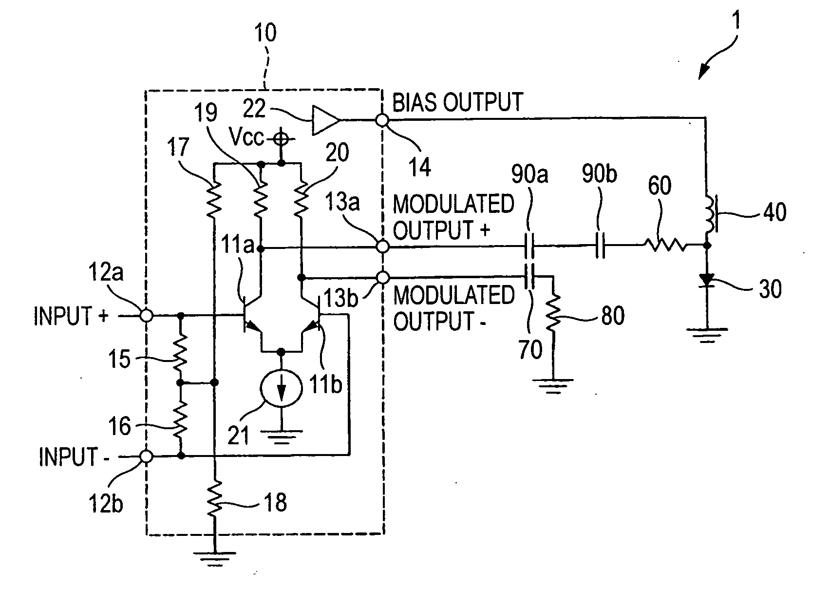
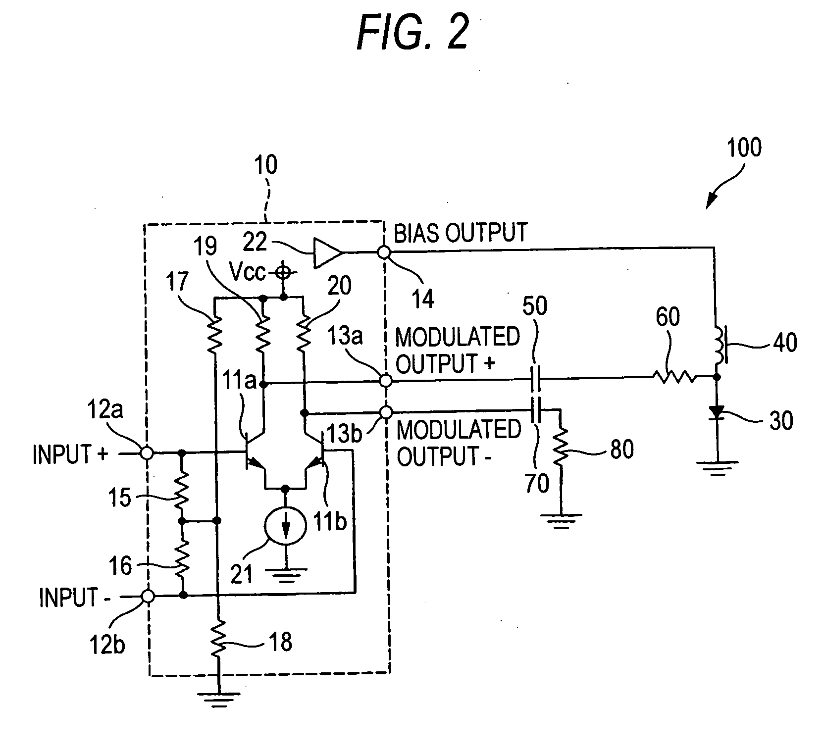
[0040]FIG. 1 shows a light emitting element driving circuit of a first embodiment of the invention. The light emitting element driving circuit 1 includes the laser driving IC 10, the semiconductor laser 30, the ferrite beads 40, the resistor 60, the capacitor 70, and the resistor 80 which have been described with reference to FIG. 2, and further includes two AC-coupling capacitors 90a, 90b which are connected together in series between the output terminal 13a and the anode of the semiconductor laser 30.

[0041] As described above, the laser driving IC 10 is configured in the same manner as the chip set MAX3740A, and includes a pair of transistors 11a, 11b, a pair of input terminals 12a, 12b, a pair of output terminals 13a, 13b, a bias output terminal 14, resistors 15, 16, 17, 18, 19, 20, a constant current source 21, and a bias generating circuit 22.

[0042] The bias generating circuit 22 can vary the voltage to be applied to the semiconductor laser 30 in the range of a bias voltage V...

second embodiment

[0056] In a second embodiment of the invention, the semiconductor laser is arranged so that the anode of the semiconductor laser is connected to the power source Vcc, the cathode is connected to a current source to ensure a bias current, and a modulating signal from a differential pair of transistors is supplied to the cathode via plural AC-coupling capacitors which are connected together in series. Also in the embodiment, even when one of the AC-coupling capacitors is short-circuited, an excessive current can be prevented from flowing through the current source.

third embodiment

[0057] A third embodiment of the invention is formed by adding an interlock mechanism to the first and second embodiments. The interlock mechanism is configured in the following manner. A switch or the like is added to a connector (not shown) through which the semiconductor laser 30 is connected to an optical waveguide such as a 25 fiber optics. When the connector is disengaged from the optical waveguide, the switch detects the disengaged state, and the laser output is interrupted or the operation of the semiconductor laser 30 is halted, whereby the optical output can be prevented from leaking to the outside.

[0058] According to the third embodiment, even when the two AC-coupling capacitors 90a, 90b enter a short-circuit state and a DC voltage is applied from the output terminal 13a to the anode of the semiconductor laser 30, the output of the semiconductor laser 30 can be prevented from being excessively increased. Therefore, the safety of the laser output can be enhanced.

Other Em...


PUM


Abstract

A light emitting element driving circuit includes: plural AC-coupling capacitors which are connected together in series; and a bias generating circuit which generates a bias current, wherein a light emitting element is driven by superposing a modulating current to the bias current via the plural AC-coupling capacitors.

Description

BACKGROUND OF THE INVENTION [0001] 1. Field of the Invention [0002] The present invention relates to a light emitting element driving circuit which drives a light emitting element such as a semiconductor laser by superposing a modulating current to a bias current, and an optical transmission apparatus, a laser printer, and a laser writing apparatus which use the light emitting element driving circuit. [0003] 2. Background Art [0004] In an optical transmission system such as an optical LAN, for example, used is an optical transmission module which drives a semiconductor laser to emit a laser beam, and which superposes a modulating current to the semiconductor laser to produce a modulated beam. [0005] As a light emitting element driving circuit used in an optical transmission module, for example, a circuit is known in which a semiconductor laser serving as a light emitting element is connected to a bias generating circuit, a predetermined bias current is supplied to the semiconductor ...

Claims


Application Information

Patent Timeline
Patent Type & Authority Applications(United States)
IPC IPC(8): H01S3/00
CPCH01S5/0427H01S5/183H04B10/504H04B10/564
Inventor BABA, TOMOKYOZUKA, SHINYAMORI, HISAYOSHISUZUKI, KAZUHIROOZEKI, SHINOBUNIITSU, TAKEHIROYAMADA, HIDENORIFUNADA, MASAO
Owner FUJIFILM BUSINESS INNOVATION CORP
Learn More