Semiconductor optical device
- Summary
- Abstract
- Description
- Claims
- Application Information
AI Technical Summary
Benefits of technology
Problems solved by technology
Method used
Image

Examples
first embodiment
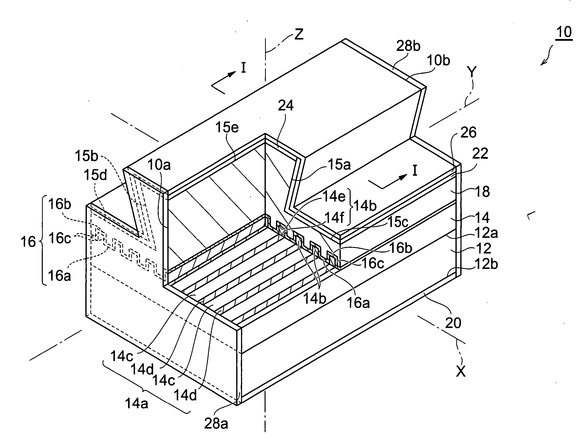
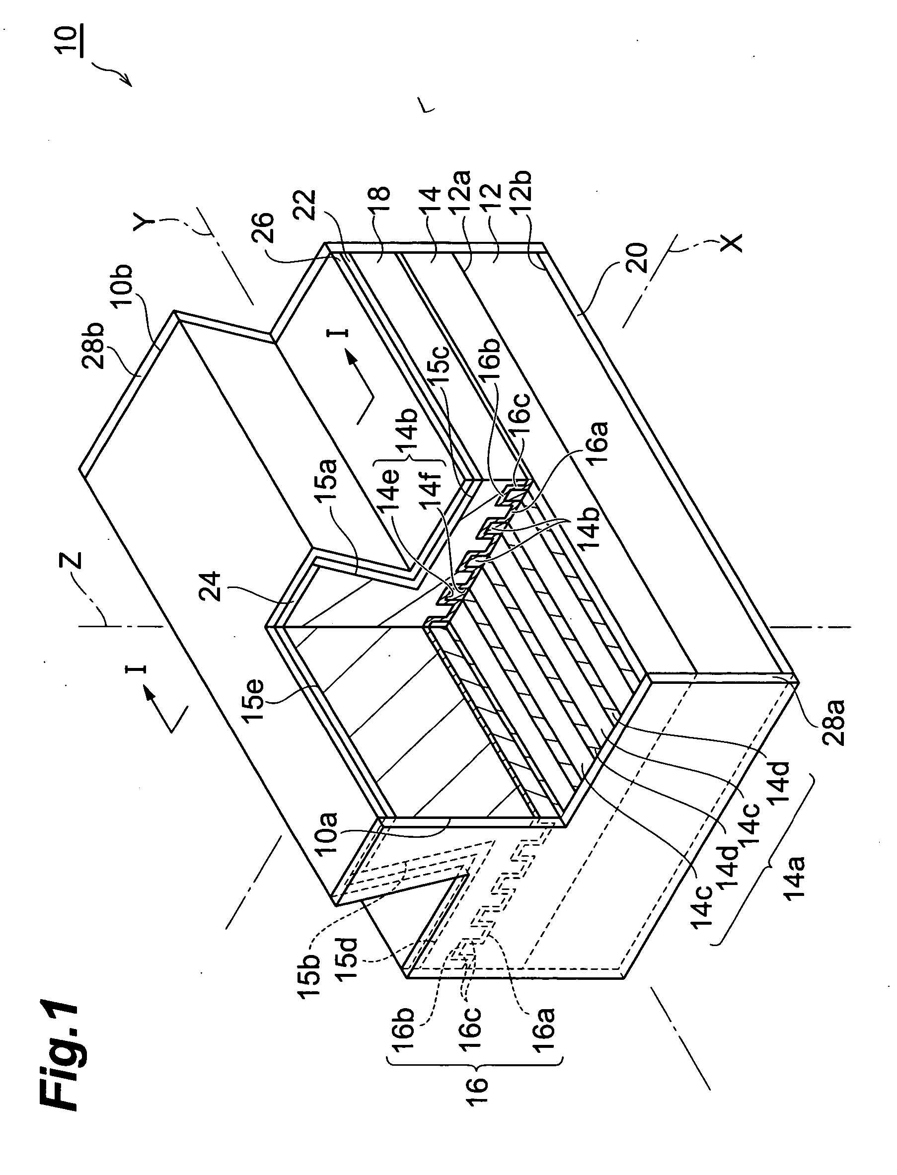
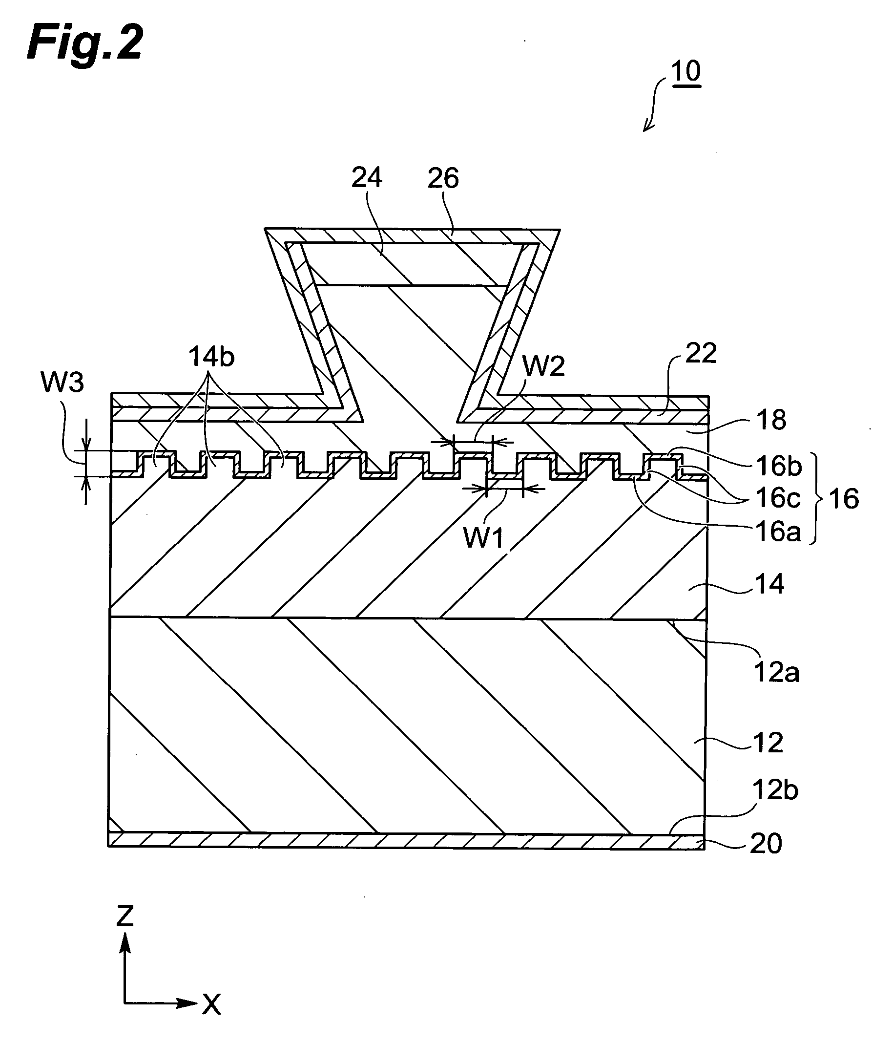
[0023]FIG. 1 is a perspective view partly in section showing a semiconductor optical amplifier according to the first embodiment of the present invention. FIG. 2 is a cross sectional view, taken along I-I line in FIG. 1, showing the semiconductor optical amplifier according to the first embodiment of the present invention. Referring to FIGS. 1 and 2, a semiconductor optical amplifier 10 includes a semiconductor substrate 12, a lower cladding layer 14, an active layer 16 and an upper cladding layer 18. Light in the active layer 16 propagates in a propagation direction, for example, the Y direction in FIG. 1.
[0024] The semiconductor substrate 12 is made of a first conductive type semiconductor, such as GaAs, and has a primary surface 12a and a backside 12b which intersect with a predetermined axis, for example, the Z-axis shown in FIG. 1.
[0025] On the primary surface 12a of the semiconductor substrate 12, the lower cladding layer 14, the active layer 16 and the upper cladding layer ...
second embodiment
[0038] A semiconductor optical amplifier according to the second embodiment will be described below. FIG. 3 is a cross-sectional view showing the semiconductor optical amplifier. The structure of the semiconductor optical amplifier 11 is the same as the above semiconductor optical amplifier 10 except for the following.
[0039] First, the semiconductor optical amplifier 11 has a first optical confinement layer 32 provided between the lower cladding layer 14 and the active layer 16, and a second optical confinement layer 34 provided between the upper cladding layer 18 and the active layer 16.
[0040] The first optical confinement layer 32 has a bandgap energy between that of the lower cladding layer 14 and that of the active layer 16, and has a refractive index between that of the lower cladding layer 14 and that of the active layer 16.
[0041] The second optical confinement layer 34 has a bandgap energy between that of the upper cladding layer 18 and that of the active layer 16, and has...
PUM
 Abstract
Description
Claims
Application Information
 - Generate Ideas
- Intellectual Property
- Life Sciences
- Materials
- Tech Scout
- Unparalleled Data Quality
- Higher Quality Content
- 60% Fewer Hallucinations
Browse by: Latest US Patents, China's latest patents, Technical Efficacy Thesaurus, Application Domain, Technology Topic, Popular Technical Reports.
© 2025 PatSnap. All rights reserved.Legal|Privacy policy|Modern Slavery Act Transparency Statement|Sitemap|About US| Contact US: help@patsnap.com