Multilevel storage nonvolatile semiconductor memory device enabling high-speed data reading and high-speed data writing

a nonvolatile semiconductor and memory device technology, applied in the direction of digital storage, instruments, computing, etc., can solve the problems of serious speed degradation, and achieve the effect of reducing the data input tim

Inactive Publication Date: 2006-09-07
RENESAS ELECTRONICS CORP
View PDF5 Cites 4 Cited by
  • Summary
  • Abstract
  • Description
  • Claims
  • Application Information

AI Technical Summary

Benefits of technology

[0072] Accordingly, a principal advantage of the present invention resides in that multivalued data stored in a single memory cell is generated from data transferred at different timings and hence data can be output every time each bit data is defined in a read operation, for reducing the data output time.
[0073] Another advantage of the present invention resides in that multivalued data stored in a single memory cell is generated from data transferred at different timings and hence data can be written every time each bit data is defined in a write operation, for reducing the data input time.

Problems solved by technology

This problem of deterioration of the speed gets serious as the number of values is increased.

Method used


Image

  • Multilevel storage nonvolatile semiconductor memory device enabling high-speed data reading and high-speed data writing
  • Multilevel storage nonvolatile semiconductor memory device enabling high-speed data reading and high-speed data writing
  • Multilevel storage nonvolatile semiconductor memory device enabling high-speed data reading and high-speed data writing

Examples


first embodiment

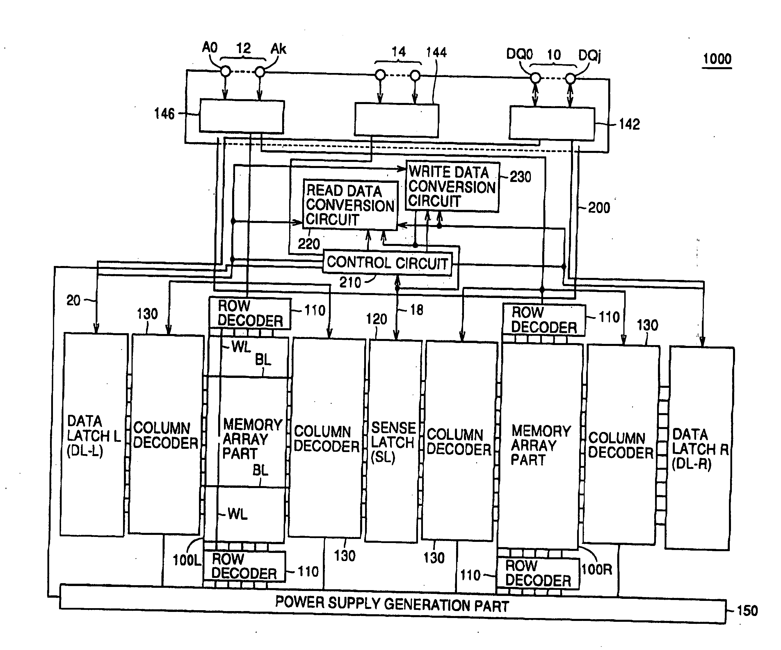
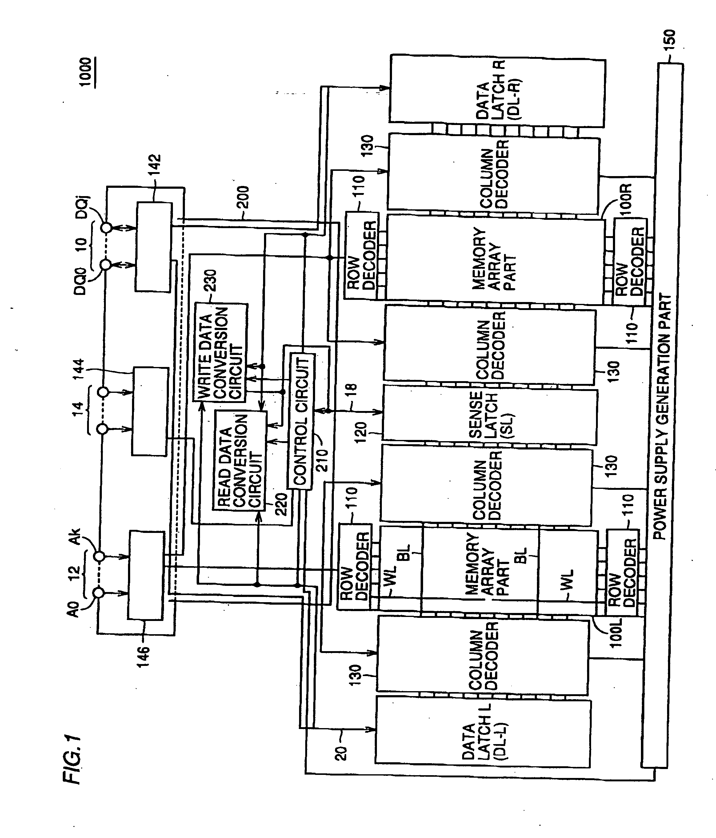
[0204]FIG. 1 is a schematic block diagram showing the structure of a flash memory 1000 forming a nonvolatile semiconductor memory device according to a first embodiment of the present invention.

[0205] A memory cell array 100 has a number of memory cells including floating gates and control gates. Also in FIG. 1, the memory cell array 100 is divided into two memory cell blocks 100R and 100L.

[0206] The control gates, drains and sources of the memory cells are connected to word lines WL, bit lines BL and source lines SCL (not shown) respectively.

[0207]FIG. 1 representatively shows two word lines WL and two bit lines BL respectively.

[0208] Row decoders 110 selectively drive the word lines WL on the basis of address signals A0 to Ak externally supplied through an address signal input terminal group 12 and an address buffer 146. A sense latch circuit 120 is provided on single ends of the bit lines BL. The bit lines BL are selected on the basis of selection signals output from column d...

second embodiment

[0279]FIGS. 16A and 16B illustrate the concept of a system of switching connection between a sense latch circuit 120 and bit lines BL1 and BL2 of a flash memory according to a second embodiment of the present invention. Referring to FIG. 16A, the bit line BL1 is connected to a sense latch SL corresponding to 1-bit data in the sense latch circuit 120. Referring to FIG. 16B, the bit line BL2 is connected to the aforementioned sense latch SL.

[0280] The flash memory according to the second embodiment is basically similar in structure to the flash memory 1000 according to the first embodiment except the structure shown in FIGS. 16A and 16B and a control operation of a control circuit 210.

[0281] When the sense latch circuit 120 captures data from the bit lines in a divided manner as to adjacent memory cells while a single word line WL is selected, first to third processing steps can be dividedly performed in parallel with each other every data reading from the memory cells due to the st...

third embodiment

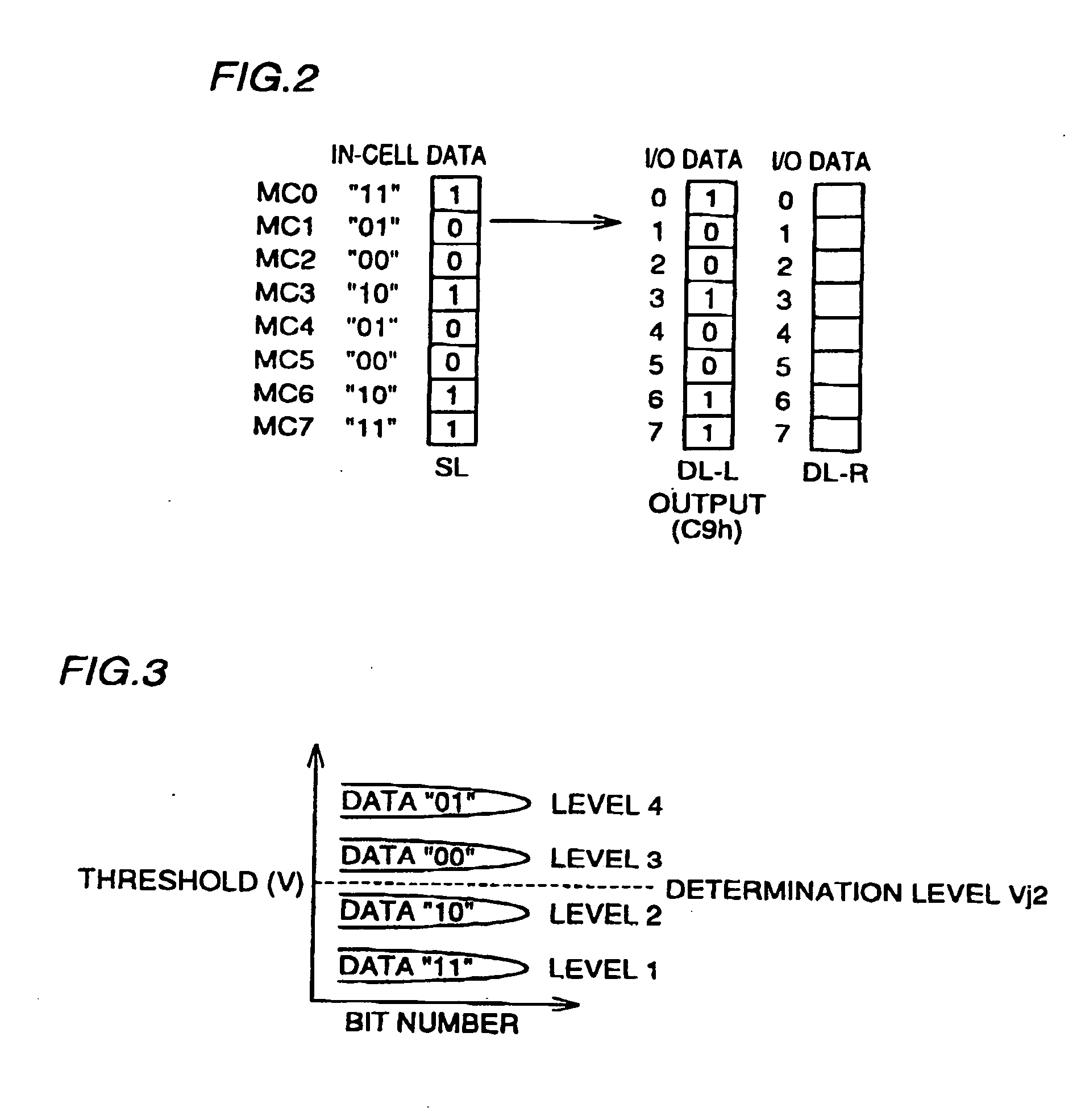
[0331] An exemplary data write operation in the structure of the flash memory 1000 according to the first embodiment is now described as a third embodiment of the present invention.

[0332] FIGS. 31 to 36, illustrating operations of the third embodiment of the present invention, are conceptual diagrams showing data held in data latches DL-L and DL-R and a sense latch SL as well as thresholds of memory cells and determination levels in writing in first to third processing steps of a write operation.

[0333]FIG. 31 shows data held in the respective latches in the first processing step of the write operation, and FIG. 32 shows thresholds of the memory cells and determination levels in the first processing step of the write operation.

[0334]FIG. 33 shows data held in the respective latches in the second processing step of the write operation, and FIG. 34 shows thresholds of the memory cells and determination levels in the second processing step of the write operation.

[0335]FIG. 35 shows ...


PUM


Abstract

A nonvolatile semiconductor memory device transmits / receives data to / from a data input / output terminal every j bits (e.g., eight bits). Each of memory cells in a memory cell array can hold data of n bits in correspondence to 2n threshold levels. A write data conversion circuit generates write data from bit data input from the same data input / output terminal in a set of a plurality of data of j bits input at different timings.

Description

BACKGROUND OF THE INVENTION [0001] 1. Field of the Invention [0002] The present invention relates to a nonvolatile semiconductor memory device, and more particularly, it relates to the structure of a nonvolatile semiconductor memory device capable of storing information of at least four values (information of at least two bits) in a single memory cell. More specifically, the present invention relates to the structure of an electrically reloadable nonvolatile semiconductor memory device such as a flash memory, for example. [0003] 2. Description of the Prior Art [0004] In order to meet increase of the storage capacity of a nonvolatile semiconductor memory device such as a flash memory, a structure capable of storing multivalued data exceeding binary data in a single memory cell has been developed. [0005]FIG. 118 is a schematic block diagram showing the overall structure of a conventional AND flash memory 8000. [0006] A memory cell array 100 includes a number of memory cells having flo...

Claims


Application Information

Patent Timeline
Patent Type & Authority Applications(United States)
IPC IPC(8): G06F12/00G11C16/02G11C11/56
CPCG11C11/5621G11C11/5628G11C11/5642
Inventor KUNORI, YUICHI
Owner RENESAS ELECTRONICS CORP
Why Eureka
Try Eureka