Split gate non-volatile memory devices and methods of forming same

Inactive Publication Date: 2006-09-14
SAMSUNG ELECTRONICS CO LTD
View PDF9 Cites 30 Cited by
  • Summary
  • Abstract
  • Description
  • Claims
  • Application Information

AI Technical Summary

Benefits of technology

[0018] In general, exemplary embodiments of the invention include non-volatile memory devices and methods for fabricating non-volatile memory devices. More specifically, exemplary embodiments of t

Problems solved by technology

1A can suffer performance problems with respect to data retention and cycling endurance.
Over time, the continuous application of such high voltage to the control gate (16) can adversely affect and stress the dielectric material of the tunneling layer (19) causing defects that can lead to unpredictable device reliability, especially for thin tunnel

Method used


Image

  • Split gate non-volatile memory devices and methods of forming same
  • Split gate non-volatile memory devices and methods of forming same
  • Split gate non-volatile memory devices and methods of forming same

Examples


Embodiment Construction

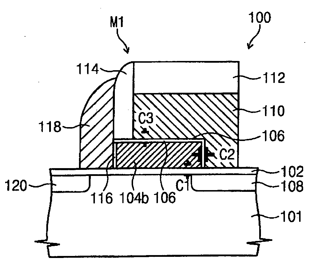
[0031] Exemplary embodiments of the invention will now be described more fully with reference to the accompanying drawings in which it is to be understood that the thickness and dimensions of the layers and regions are exaggerated for clarity. It is to be further understood that when a layer is described as being “on” or “over” another layer or substrate, such layer may be directly on the other layer or substrate, or intervening layers may also be present. Moreover, similar reference numerals used throughout the drawings denote elements having the same or similar functions.

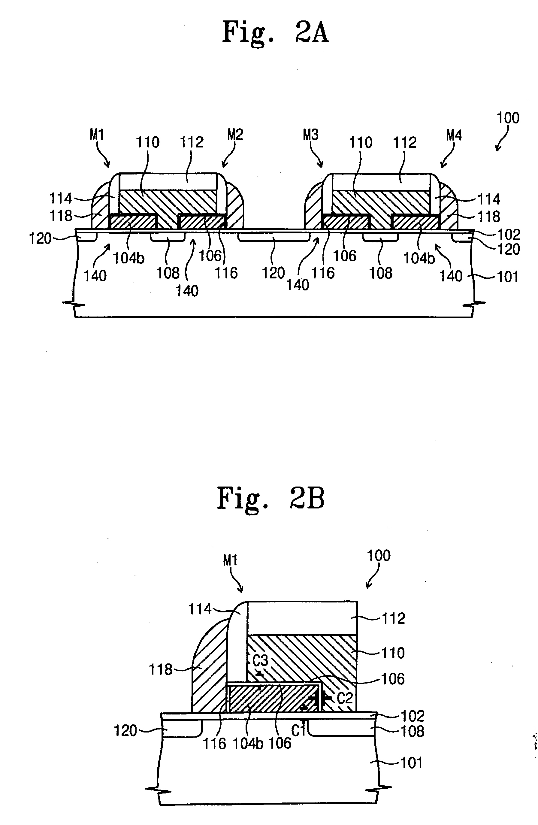
[0032]FIGS. 2A and 2B are cross-sectional schematic views of a split gate non-volatile memory device (100) according to an exemplary embodiment of the invention. In particular, FIG. 2A depicts two pairs of split-gate memory cells M1 / M2 and M3 / M4 formed on a p-type semiconductor substrate layer (101). A plurality of diffusion regions (108) and (120) are formed in the substrate (101). In particular, in one exemplar...


PUM


Abstract

Non-volatile memory devices and methods for fabricating non-volatile memory devices are disclosed. More specifically, split gate memory devices are provided having frameworks that provide increased floating gate coupling ratios, thereby enabling enhanced programming and erasing efficiency and performance.

Description

CROSS-REFERENCE TO RELATED APPLICATION [0001] This application claims priority to Korean Patent Application No. 2005-0021074, filed on Mar. 14, 2005, which is incorporated herein by reference. TECHNICAL FIELD OF THE INVENTION [0002] The present invention relates generally to non-volatile memory devices and methods for fabricating non-volatile memory devices. More specifically, the present invention relates to split gate memory devices having frameworks that provide increased floating gate coupling ratios, thereby enabling enhanced programming and erasing efficiency and performance. BACKGROUND [0003] In general, non-volatile memory devices are memory devices that will retain stored data even while power is off. Typically, non-volatile memory devices are utilized in various products and devices, such as mobile telecommunication devices, memory cards, smart cards, and other devices and applications where power is not always available, frequently interrupted and / or when lower power usag...

Claims


Application Information

Patent Timeline
IPC IPC(8): H01L29/788H01L21/8238
CPCH01L21/28273H01L27/115H01L27/11521H01L29/42328H01L29/7885H01L29/40114H10B69/00H10B41/30H01L29/66825
Inventor JEON, HEE SEOGKANG, SUNG-TAEGKWON, HYOK-KIKIM, YONG TAESEO, BOYOUNGYOON, SEUNG BEOMHAN, JEONG-UK
Owner SAMSUNG ELECTRONICS CO LTD
Why Eureka
Try Eureka