Method and structure to provide balanced mechanical loading of devices in compressively loaded environments

a technology of mechanical loading and devices, applied in semiconductor devices, semiconductor/solid-state device details, cooling/ventilation/heating modification, etc., can solve the problems of deformation of the substrate, non-uniform lga loading, and more difficult (and sometimes costly) the solution becomes

Inactive Publication Date: 2006-09-14
GLOBALFOUNDRIES INC
View PDF10 Cites 35 Cited by
  • Summary
  • Abstract
  • Description
  • Claims
  • Application Information

AI Technical Summary

Benefits of technology

[0013] Another embodiment can include the compressible support tube positioned around the upper section of the alignment posts between the thermally conductive device in addition to one or mor...

Problems solved by technology

The higher the minimum load, the higher the total required load, the more challenging (and sometimes costly) the solution becomes.
However, for designs in which the die is substantially smaller in area than the substrate, placing a ...

Method used


Image

  • Method and structure to provide balanced mechanical loading of devices in compressively loaded environments
  • Method and structure to provide balanced mechanical loading of devices in compressively loaded environments
  • Method and structure to provide balanced mechanical loading of devices in compressively loaded environments

Examples


Embodiment Construction

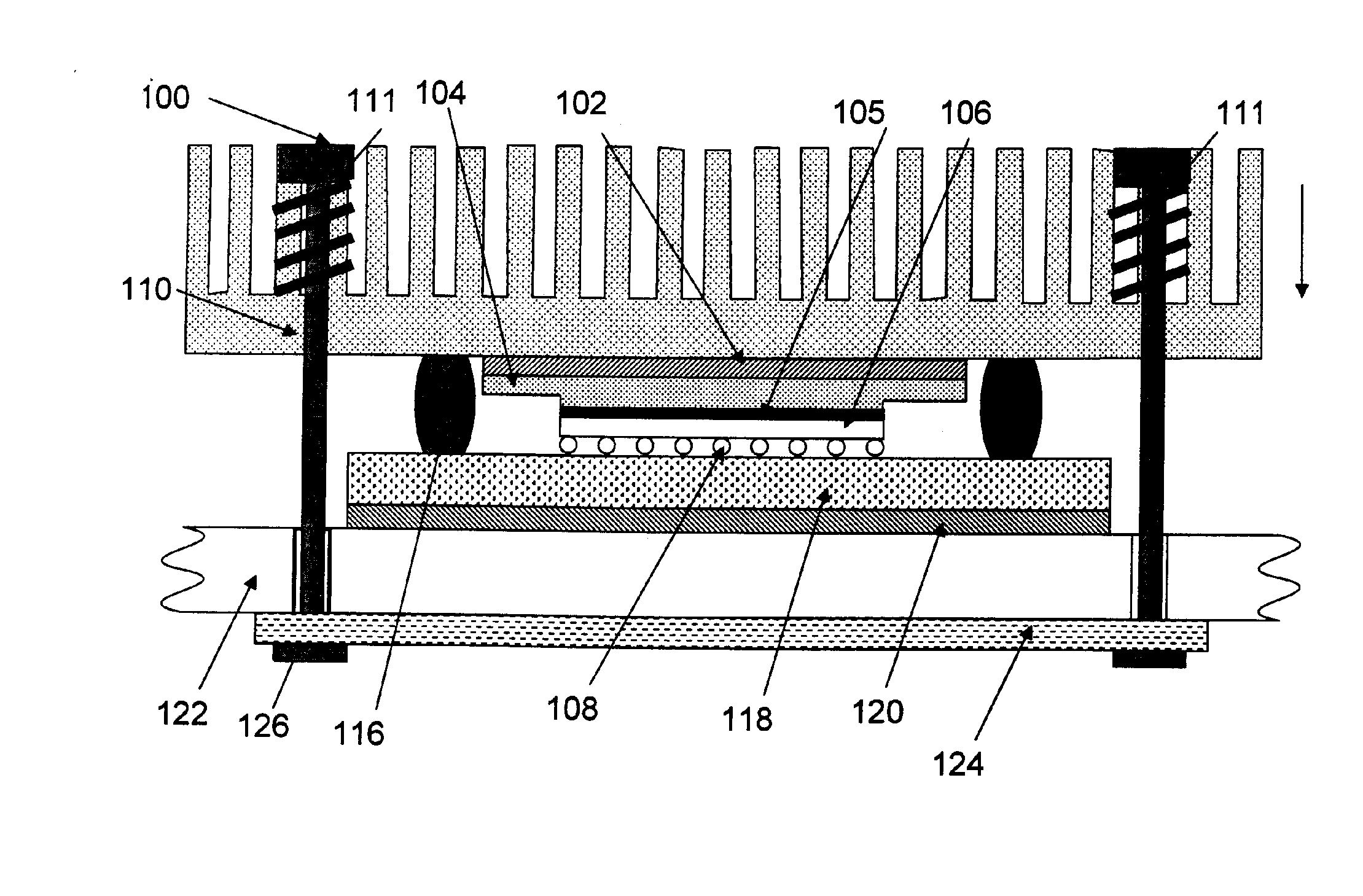
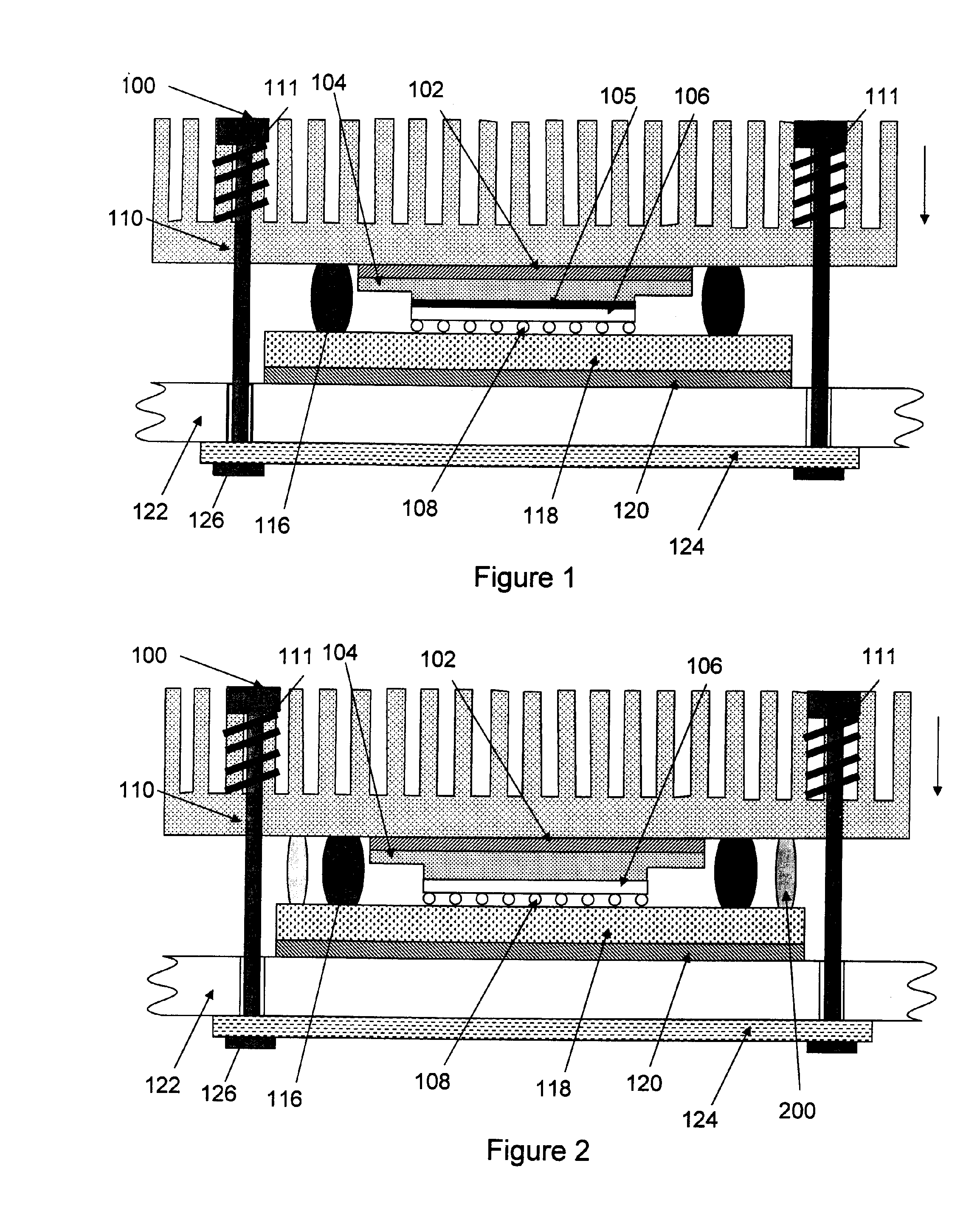
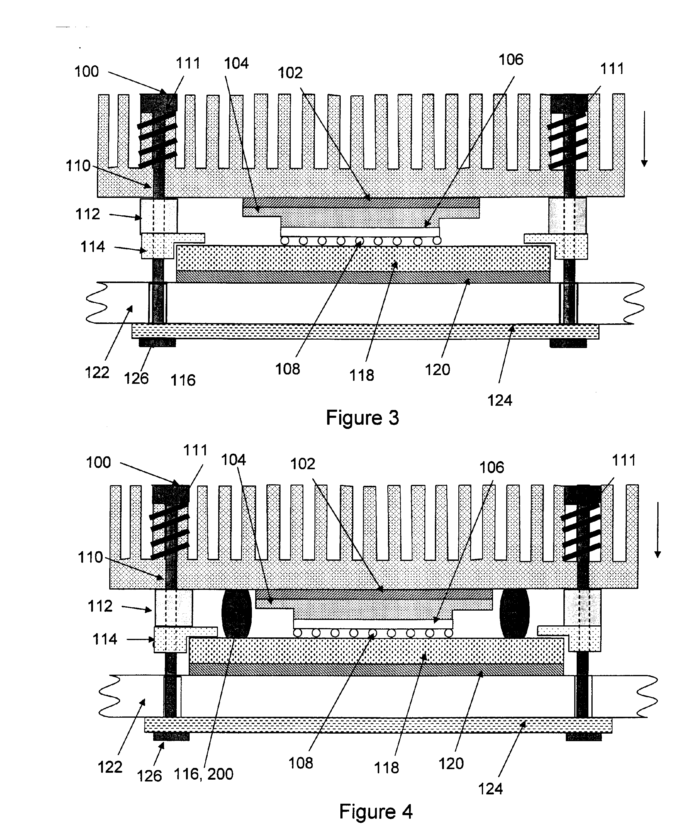
[0027] The present invention and the various features and advantageous details thereof are explained more fully with reference to the nonlimiting embodiments that are illustrated in the accompanying drawings and detailed in the following description. It should be noted that the features illustrated in the drawings are not necessarily drawn to scale. Descriptions of well-known components and processing techniques are omitted so as to not unnecessarily obscure the present invention. The examples used herein are intended merely to facilitate an understanding of ways in which the invention may be practiced and to further enable those of skill in the art to practice the invention. Accordingly, the examples should not be construed as limiting the scope of the invention.

[0028] While the shape, position, and usage of many of the devices mentioned herein were not previously known, the methods of manufacturing and materials used to manufacture such devices has been disclosed previously. For ...


PUM


Abstract

An integrated circuit chip mounting structure includes a chip carrier electrically connected to a circuit board with an integrated circuit chip mounted on the chip carrier. In addition, a thermally conductive device is thermally connected to the chip and a set of compressible support members are provided to transmit a portion of an applied compressive load from the thermally conductive device to the chip and chip carrier.

Description

BACKGROUND OF THE INVENTION [0001] 1. Field of the Invention [0002] The invention generally relates to a structure and a method for forming an integrated circuit chip carrier structure and more particularly to an integrated circuit chip mounted on a chip carrier with a set of compressible support members that transmit force from a thermally conductive device to the chip carrier. [0003] 2. Description of the Related Art [0004] High power electronic devices are often cooled by bonding them to a good thermal conductor. In common configurations, this is accomplished by first joining the front (circuit) side of a flip chip to a substrate or carrier using electrical conductors (e.g., solder balls). A thermal conductor (a heat spreader or heatsink) is then bonded to the back side of the die using curable organic materials or a solder. In either case, the gap between the die and the thermal conductor should be made as thin as possible to minimize the thermal resistance path without impactin...

Claims


Application Information

Patent Timeline
IPC IPC(8): H01L23/34
CPCH01L23/4006H01L2023/405H01L2023/4062H01L2023/4081H01L2224/16H01L2224/73253H01L2224/16227H01L2924/00011H01L2924/00014H01L2224/0401
Inventor COICO, PATRICK A.EDWARDS, DAVID L.FASANO, BENJAMIN V.GOLDMANN, LEWIS S.INGALLS, ELLYN M.JUNE, MICHAEL S.TOY, HILTON T.ZUCCO, PAUL A.
Owner GLOBALFOUNDRIES INC
Why Eureka
Try Eureka