Semiconductor Package Structures Having Liquid Coolers Integrated with First Level Chip Package Modules

a technology of semiconductor package structure and liquid cooler, which is applied in the direction of semiconductor device details, semiconductor/solid-state device devices, electrical devices, etc., can solve the problems of power density, limited ability to implement chip modules with higher densities and performance, and inability to remove heat from air cooling solutions, etc., to prevent the effect of package defect mechanism and structural failur

Inactive Publication Date: 2009-11-19
GLOBALFOUNDRIES INC
View PDF12 Cites 80 Cited by
  • Summary
  • Abstract
  • Description
  • Claims
  • Application Information

AI Technical Summary

Problems solved by technology

The increased power density poses practical limitations to the level of integration density and performance that may be achieved.
Indeed, the ability to implement chip modules with higher densities and higher performance is limited primarily by the ability to effectively cool the chip modules during normal operation.
In high performance, high density chip package structures, air cooling solutions are not capable of removing heat due to very high power density or due to space and / or air flow limitations, thereby requiring liquid cooling solutions (e.g., water coolant).
More specifically, package components formed from materials having different coefficients of thermal expansion (CTE) tend to expand and contract by different amounts during thermal cycling, which is a phenomenon known as “CTE mismatch”.
A key issue with first level organic package substrates is the CTE mismatch between silicon chips (˜3 ppm / C) and the composite laminate carrier substrate (15-20 ppm / C) to which the chips are attached via C4s.
Such CTE mismatch can result in mechanical stresses on the C4 connections between the chip and the organic carrier substrate during thermal cycling.
As these mechanical stresses are applied over repeated thermal cycles, the C4 connections may become fatigued and fail.
Moreover, even when underfill material is used to maintain the structural integrity of C4 contacts, the stress generated by the CTE mismatch between the silicon chip and organic substrate, for example, can result in bowing or bending of substrates and chips.
For instance, the differences in thermal expansion between the silicon chip and the organic carrier substrate can cause the chip to warp by 60 microns or more after processing, and cause the substrate to be even more substantially warped.
Such bending / bowing can not only generate significant stresses and strains in the electrical contacts between the chip and substrate, but the chip may be subjected to a high tensile stress, so a small defect or scratch can result in chip cracking or delamination of the organic substrate layers.
This warpage resulting from CTE mismatch between silicon chip and organic carrier substrate during thermal cycling becomes worse as the chip size increases and this is particularly problematic for lidless packages where the backside surface of the chip is exposed.
The package lid (33) design can vary depending on the application but the package lid (33) design is an important consideration in the overall package framework as a package lid which is too thick and too stiff can result in excessive stress and failure in the package.
Although a lidless chip package structure (12) of FIG. 3 can theoretically provide increased thermal performance, the ability to actually achieve a low thermal resistance TIM layer (73) between the chip (32) and cooler (40) in the framework of FIG. 3 is problematic by virtue of the increased mechanical complexity of having the cooler (40) attached to the circuit board (20) and the chip (32) attached to the laminate carrier (31) which is attached to the board (20).
However, the disadvantage of using a paste or grease is its tendency to pump out from the space between the backside of the chip (32) and the cooler (40) as a result of thermal excursions where chip warpages vary due to the mechanical complexity of having the cooler (40) attached to the board (20) and the chip (32) attached to the laminate carrier (31) which is attached to the board (20).
This large size metallic cooler posed practical limitations such as follows:
When a BGA (ball grid array) or CGA (column grid array) attachment techniques are used to mechanically / electrically connect the carrier (31) to the circuit board (20), a large size metallic cooler (40) results in a large thermal mass that is not compatible with the BGA or CGA reflow process.
Moreover, the resulting weight of the SCM module may be too high preventing the module from self-aligning to the printed circuit board pads and can compress the liquid solder excessively thereby causing shorts during the solder reflow process.
For other mechanical area array connection methods such as LGA (land grid array) or a pin grid array (PGA), where a compressive force must be applied for actuation, such compressive forces may result in a thin and / or non uniform thickness of the TIM layer between the liquid cooler and chip.

Method used


Image

  • Semiconductor Package Structures Having Liquid Coolers Integrated with First Level Chip Package Modules
  • Semiconductor Package Structures Having Liquid Coolers Integrated with First Level Chip Package Modules
  • Semiconductor Package Structures Having Liquid Coolers Integrated with First Level Chip Package Modules

Examples


Embodiment Construction

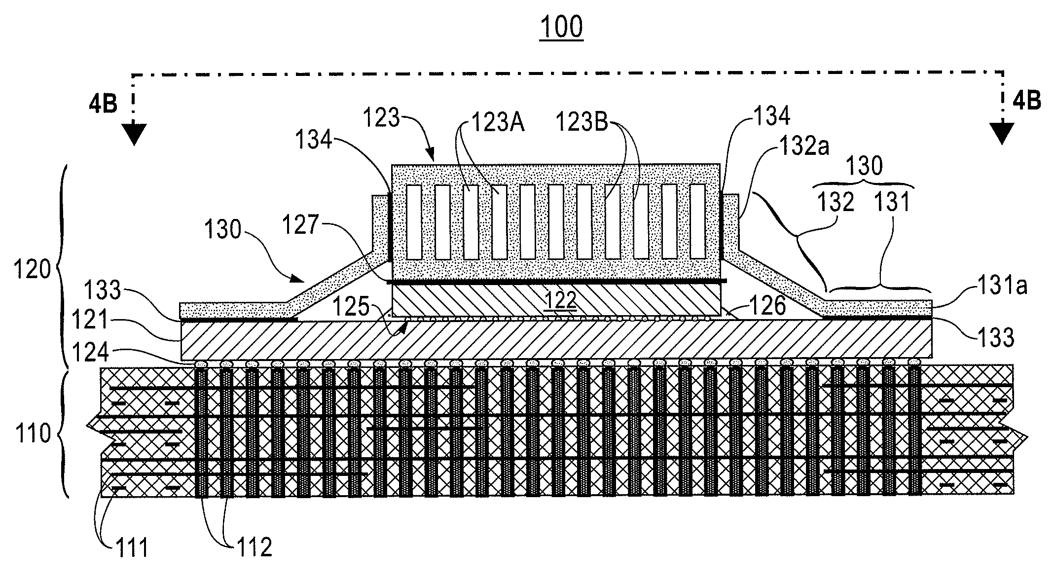
[0046]Various techniques for constructing electronic modules having chip level package structures with integrally packaged metallic liquid cooling devices will now be described in further detail with reference to exemplary embodiments discussed hereafter. In general, electronic apparatus according to exemplary embodiments of the invention include semiconductor chip modules, such as SCMs, having an IC chip flip chip mounted on a first (top side) surface of a flexible carrier substrate having an area array of electrical contacts formed on a second (bottom side) surface of the substrate opposite the first surface, a metallic cooler thermally coupled directly to a backside surface of the IC chip and a stiffener member which is (i) bonded to the first surface of the carrier substrate to provide mechanical rigidity to the carrier substrate, as well as (ii) mechanically coupled to the metallic cooler to fixedly dispose the metallic cooler device in place on the backside of the IC chip.

[004...


PUM


Abstract

Semiconductor package structures are provided which are designed to have liquid coolers integrally packaged with first level chip modules. In particular, apparatus for integrally packaging a liquid cooler device within a first level chip package structure include structures in which a liquid cooler device is thermally coupled directly to the back side of an integrated circuit chip flip-chip mounted on flexible chip carrier substrate. The liquid cooler device is mechanically coupled to the package substrate through a metallic stiffener structure that is bonded to the flexible package substrate to provide mechanical rigidity to the flexible package substrate.

Description

BACKGROUND[0001]1. Technical Field[0002]The present invention relates generally to semiconductor package structures having liquid coolers integrally packaged with first level chip modules and, more specifically, apparatus and methods for integrally packaging a liquid cooler device with in a first level chip package structure wherein the liquid cooler device is thermally coupled directly to the back side of an integrated circuit chip flip-chip mounted on flexible chip carrier substrate, and wherein the liquid cooler device is mechanically coupled to the package substrate through a metallic stiffener structure that is bonded to the flexible package substrate to provide mechanical rigidity to the flexible package substrate.[0003]2. Discussion of Related Art[0004]Technological innovations in semiconductor fabrication and packaging technologies have enabled development of high performance, and high integration density semiconductor chip modules. As chip geometries are scaled down and ope...

Claims


Application Information

Patent Timeline
Patent Type & Authority Applications(United States)
IPC IPC(8): H01L23/473
CPCH01L23/3675H01L23/473H01L2924/10253H01L2224/32245H01L2924/19105H01L2224/73253H01L2224/73204H01L2224/32225H01L23/49833H01L23/4985H01L2023/4043H01L2023/4087H01L2924/15311H01L2224/16225H01L2924/00
Inventor BEZAMA, RASCHID JOSECOLGAN, EVAN GEORGEGAYNES, MICHAELMAGERLEIN, JOHN HAROLDMARSTON, KENNETH C.WEI, XIAOJIN
Owner GLOBALFOUNDRIES INC
Why Eureka
Try Eureka