Leadless chip carrier design and structure

a chip carrier and leadless technology, applied in the field of electronic packaging, can solve the problems of increasing the speed and power consumption of semiconductor devices, limiting the properties of semiconductor devices, and electrical parasitics caused by electrical parasitics

Inactive Publication Date: 2001-02-20
SKYWORKS SOLUTIONS INC
View PDF11 Cites 75 Cited by
  • Summary
  • Abstract
  • Description
  • Claims
  • Application Information

AI Technical Summary

Problems solved by technology

However, as device sizes decrease and electrical components are moved closer together, one of the limiting properties of the semiconductor device is the electrical parasitics caused by resistance, capacitance and inductance effects.
Also, the need to control device generated heat has become more critical as the speeds and power consumption of semiconductor devices has increased.
Electrical parasitics, particularly inductance, are some of the parameters that can adversely affect the performance of electrical packages.
Another factor is the lack of a good ground plane located close to the device.
Present packages also have problems with dissipating heat.
The resulting thermal stresses can reduce the life of the semiconductor device by causing mechanical failures.

Method used


Image

  • Leadless chip carrier design and structure
  • Leadless chip carrier design and structure
  • Leadless chip carrier design and structure

Examples


Embodiment Construction

The present invention provides for a more efficient electronic device particularly suited for radio frequency (RF) applications by minimizing electrical parasitics and providing for predictable electrical and thermal performance. The electronic device in accordance with the invention is especially applicable to devices with up to approximately 64 leads, which is particularly suited to many RF and analog applications, but it will be readily appreciated that the following description also applies to packages of different sizes and different number of I / O pins.

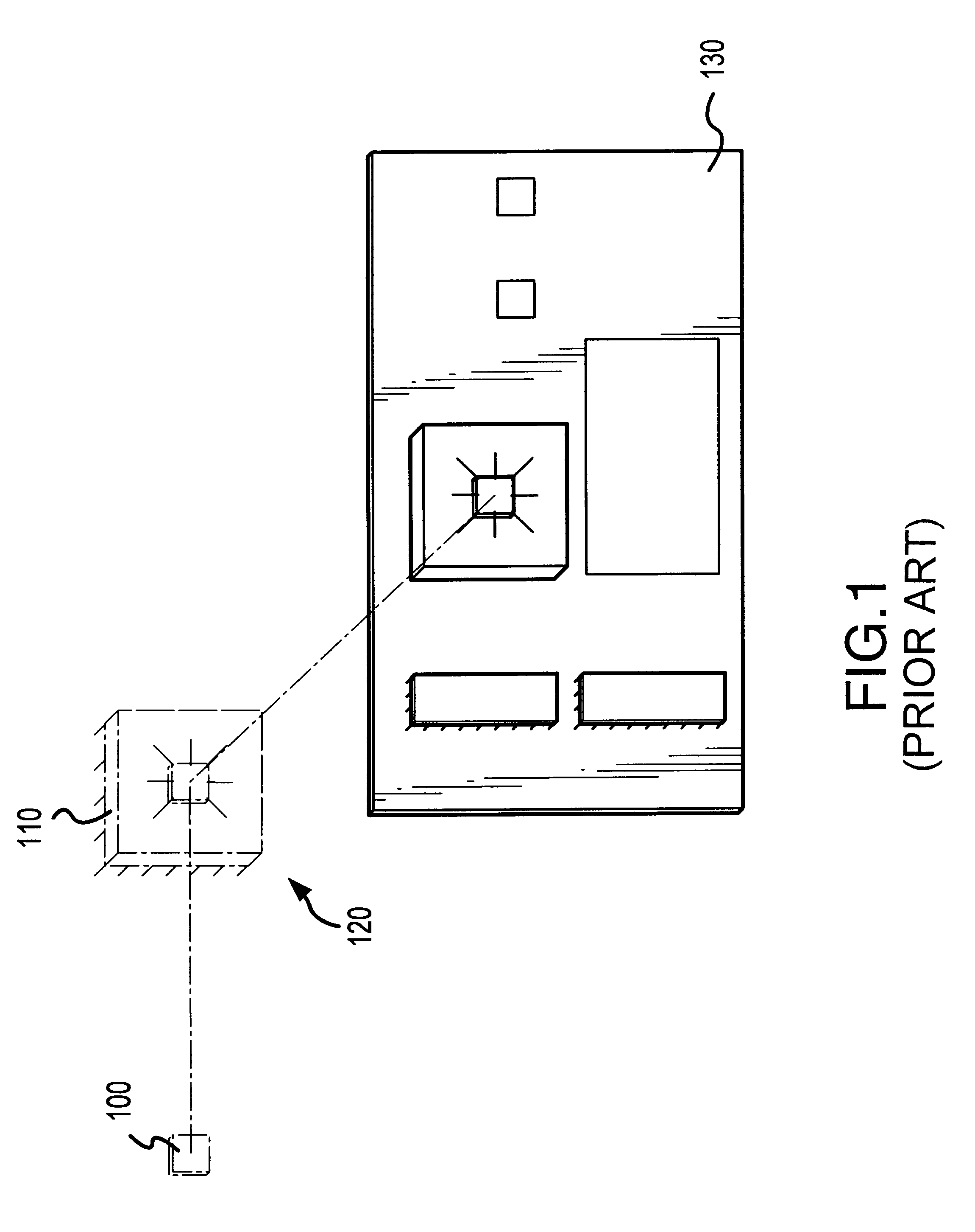
Referring now to FIG. 1, an electronic packaging hierarchy is illustrated. A semiconductor device chip 100 is mounted on an electronic package 110 to form a semiconductor device 120. The resulting semiconductor device can be connected to a printed circuit board 130 that is plugged into a mother board (not shown).

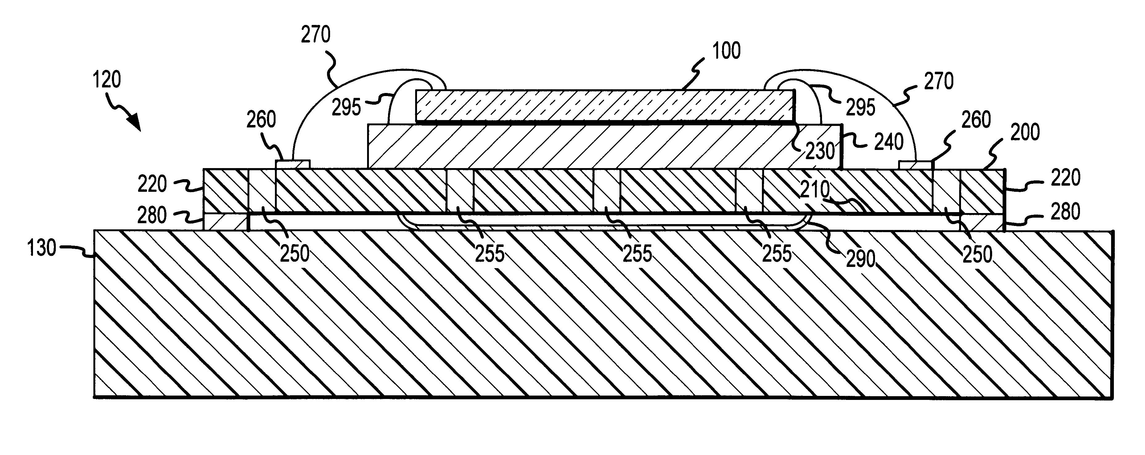
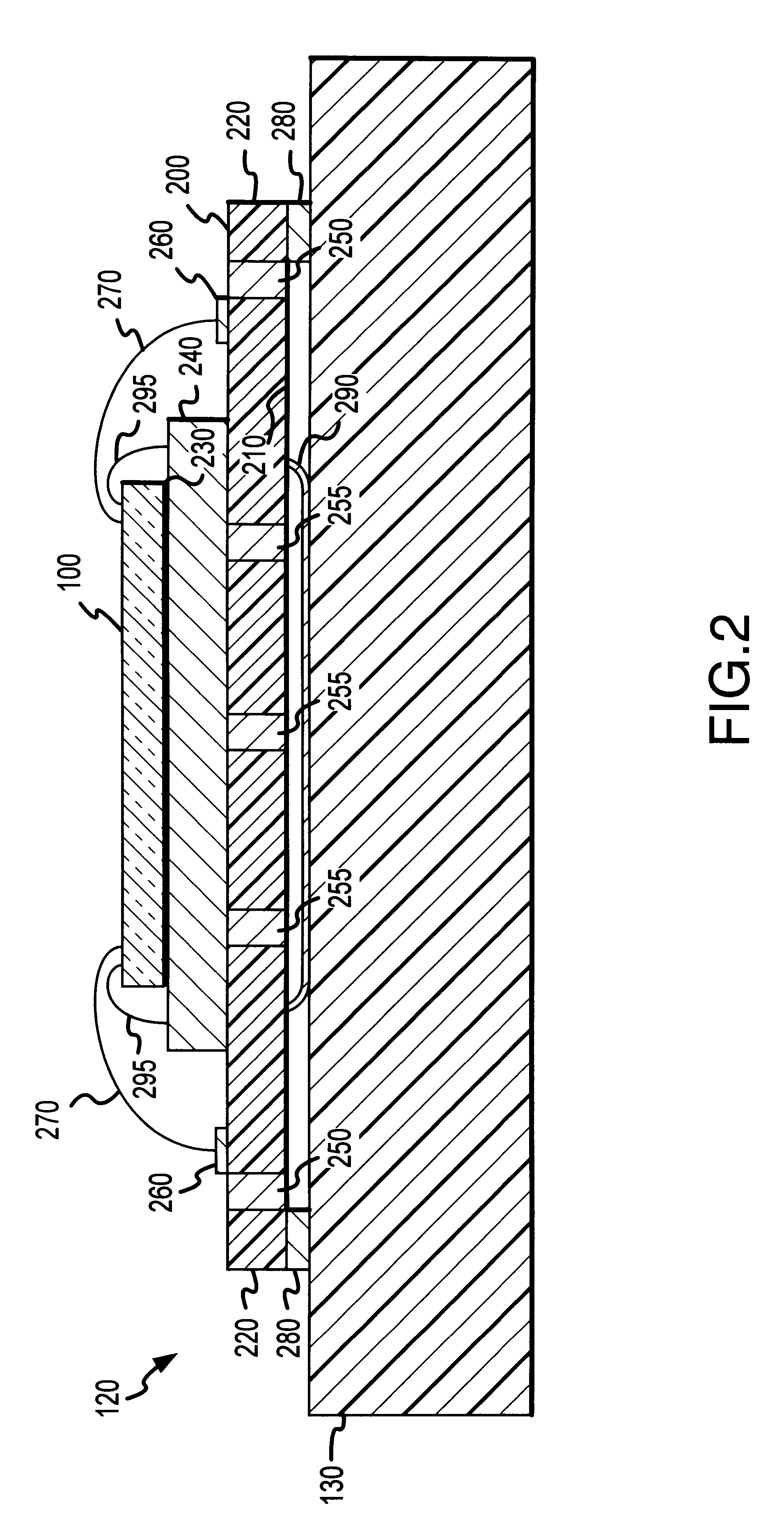
FIG. 2 illustrates in cross-section, a semiconductor device 120 in accordance with a preferred embodiment of the presen...


PUM


Abstract

A semiconductor device is provided in the form of a chip carrier (e.g., chip / IC scale carrier for RF applications) that includes an integrated circuit chip attached to a die attach pad. The device has an interconnect substrate having an upper surface and a lower surface, with a plurality of vias passing through the thickness of the interconnect substrate from the upper surface to the lower surface. The die attach pad is located on the upper surface of the interconnect substrate, and a heat spreader is located on the lower surface of the interconnect substrate. A first group of vias is positioned to intersect both the die attach pad and the heat spreader. A second group of vias is positioned away from the die attach pad and the heat spreader. The upper surface has a plurality of bond pads that are abutting the second group of vias and the lower surface has a plurality of lands that are also abutting the second group of vias.

Description

1. Field of the InventionThe present invention generally relates to electronic packaging, and more particularly, to a leadless chip carrier design and structure.2. Description of the Related ArtThe microelectronics industry has continued to make significant advances in semiconductor device technology. Semiconductor devices are getting smaller, more dense, and run at higher speeds. However, as device sizes decrease and electrical components are moved closer together, one of the limiting properties of the semiconductor device is the electrical parasitics caused by resistance, capacitance and inductance effects. This is particularly troubling in radio frequency (RF) devices, where it is important to minimize electrical parasitics and to be able to predict their effects reliably. Also, the need to control device generated heat has become more critical as the speeds and power consumption of semiconductor devices has increased.Controlling electrical parasitics is also important at the pac...

Claims


Application Information

Patent Timeline
Patent Type & Authority Patents(United States)
IPC IPC(8): H01L23/367H01L23/34H01L23/64H01L23/58
CPCH01L23/3677H01L23/64H01L2224/48235H01L2224/48237H01L2924/01079H01L2924/30107H01L24/48H01L2224/73265H01L24/45H01L2224/05599H01L2224/45124H01L2224/45144H01L2224/45147H01L2224/85424H01L2224/85444H01L2224/8547H01L2924/14H01L2924/00014H01L2924/00H01L23/48
Inventor HASHEMI, HASSAN S.
Owner SKYWORKS SOLUTIONS INC
Why Eureka
Try Eureka