Method of making a circuitized substrate having at least one capacitor therein

a technology of circuitized substrates and capacitors, which is applied in the direction of fixed capacitors, fixed capacitor details, thin/thick film capacitors, etc., can solve the problems of many manufacturing problems, inability to afford the pcb external surface area real estate savings, and fibrous materials occupying a relatively significant portion of the substrate's total volume, so as to enhance the circuitized substrate art

Inactive Publication Date: 2008-10-09
ENDICOTT INTERCONNECT TECH
View PDF15 Cites 83 Cited by
  • Summary
  • Abstract
  • Description
  • Claims
  • Application Information

AI Technical Summary

Benefits of technology

[0047]It is, therefore, a primary object of the present invention to enhance the circuitized substrate a

Problems solved by technology

Typically, these discrete passive devices occupy a high percentage of the surface area of the completed multi-layered substrate, which is obviously undesirable from a future design perspective due to the ever-present demand for miniaturization.
With respect to the following patents, some mention or suggest problems associated with the methods and resulting materials used to do so.
That is, the resulting PCB still requires the utilization of external devices thereon, and thus does not afford the PCB external surface area real estate savings mentioned above which are desired and demanded in today's technology.
Unfortunately, in doing so, they also confront many manufacturing problems.
Such fibrous materials occupy a relatively significant portion of the substrate's total volume, a disadvantage especially when attempting to produce highly dense numbers of thru-holes and very fine line circuitry to meet new, more stringent design requirements.
If the glass is not removed, a loss of continuity might occur in the internal wall metal deposit.
In addition, both continuous and semi-continuous glass fibers add weight and thickness to the overall final structure, yet another disadvantage associated with such fibers.
Additionally, since lamination is typically at a temperature above 150 degrees C., the resinous portion of the laminate may then shrink during cooling to the extent permitted by the rigid copper cladding, which is not the case for the continuous strands of fiberglass or other continuous reinforcing material used.
The strands thus take on a larger portion of the substrate's volume following such shrinkage and add further to complexity of manufacture in a high-density product.
Obviously, this problem is exacerbated as feature sizes (line widths and thicknesses, and thru-hole diameters) decrease.
Consequently, even further shrinkage may occur.
The shrinkage, possibly in part due to the presence of the relatively large volume percentage of continuous or semi-continuous fiber strands in the individual layers used to form a final product possessing many such layers, may have an adverse affect on dimensional stability and registration between said layers, adding even more problems for the PCB manufacturer.
The presence of glass fibers, especially those of the woven type, also substantially impairs the ability to form high quality, very small thru-holes, including when using a laser.
This wide variation in encountered glass density leads to problems obtaining the proper laser power for each thru-hole and may result in wide variations in thru-hole quality, obviously unacceptable by today's very demanding man

Method used


Image

  • Method of making a circuitized substrate having at least one capacitor therein
  • Method of making a circuitized substrate having at least one capacitor therein
  • Method of making a circuitized substrate having at least one capacitor therein

Examples


example one

[0103]38.5 grams (gm) of epoxy novolac resin (e.g., one sold under product designation “LZ 8213” by Huntsman, having a business location at 500 Huntsman Way, Salt Lake City, Utah) containing about 35 percent by weight methyl ethyl ketone, and catalyzed with about 0.015 parts per hundred (PPH) of 2-methyl-imidazole and 12.8 gm of a high molecular weight, reactive thermoplastic phenoxy resin (e.g., the aforementioned one sold under the product name “PKHS-40” by the InChem Corporation) containing 60 percent by weight methyl ethyl ketone, may be mixed together with 100 gm of barium titanate (BaTiO3) powder (available from Cabot Corporation, having a business location in Boyertown, Pa.). The barium titanate powder may include a mean particle size of 0.12 microns and a surface area of 8.2 m2 / gm. Also mixed in with this composition may be 20 gm of methyl ethyl ketone. The composition may then be ball milled for one day, after which a thin coating of this well dispersed composition may be d...

example two

[0104]50 gm of epoxy novolac resin (e.g., the “LZ 8213” above by Huntsman, containing about 35 percent by weight methyl ethyl ketone and catalyzed with about 0.015 PPH of 2-methyl-imidazole, and 19.2 gm of the high molecular weight, reactive thermoplastic phenoxy resin “PKHS-40” (containing 60 percent by weight methyl ethyl ketone), may be mixed together with 111 gm of barium titanate (BaTiO3) powder from Cabot Corporation having the same mean particle size and surface area as in Example One (0.12 microns and 8.2 m2 / gm, respectively). Also mixed in with this composition may be 20 gm of methyl ethyl ketone. As also in Example One, the composition may then be ball milled for one day. A thin coating of the composition may then be deposited on a dielectric substrate layer and dried at about 130 degrees C. for three minutes in a standard convection oven. As in Example One, this heating will serve to substantially remove all residual organic solvents. Following removal and cooling to room...

example three

[0105]50 gm of epoxy novolac resin (e.g., the “LZ 8213” above by Huntsman), containing about 35 percent by weight methyl ethyl ketone and catalyzed with about 0.015 PPH of 2-methyl-imidazole, and 19.2 gm of the high molecular weight, reactive thermoplastic phenoxy resin “PKHS-40” (containing 60 percent by weight methyl ethyl ketone), may be mixed together with 111 gm of barium titanate (BaTiO3) powder from Cabot Corporation having the same mean particle size and surface area as in Example One (0.12 microns and 8.2 m2 / gm, respectively). Also mixed in with this composition may be 20 gm of methyl ethyl ketone. As also in Example One, the composition may then be ball milled for one day. Around 25 microns thick coating of the composition may then be deposited on a two-ounce smooth Cu foil (carrier sheet) and dried at about 130 degrees C. for three minutes in a standard convection oven. As in Example One, this heating will serve to substantially remove all residual organic solvents. Follo...


PUM


Abstract

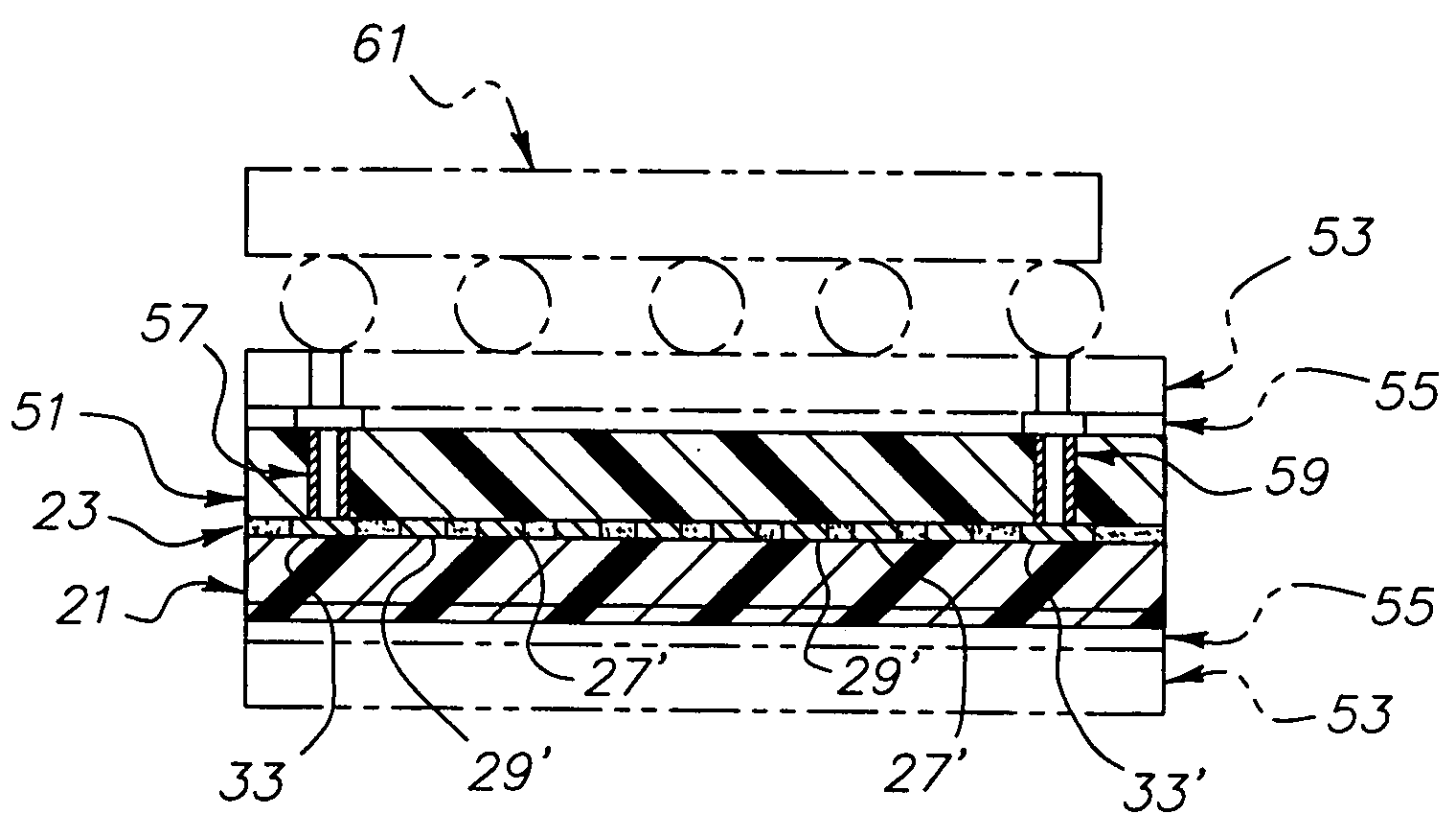
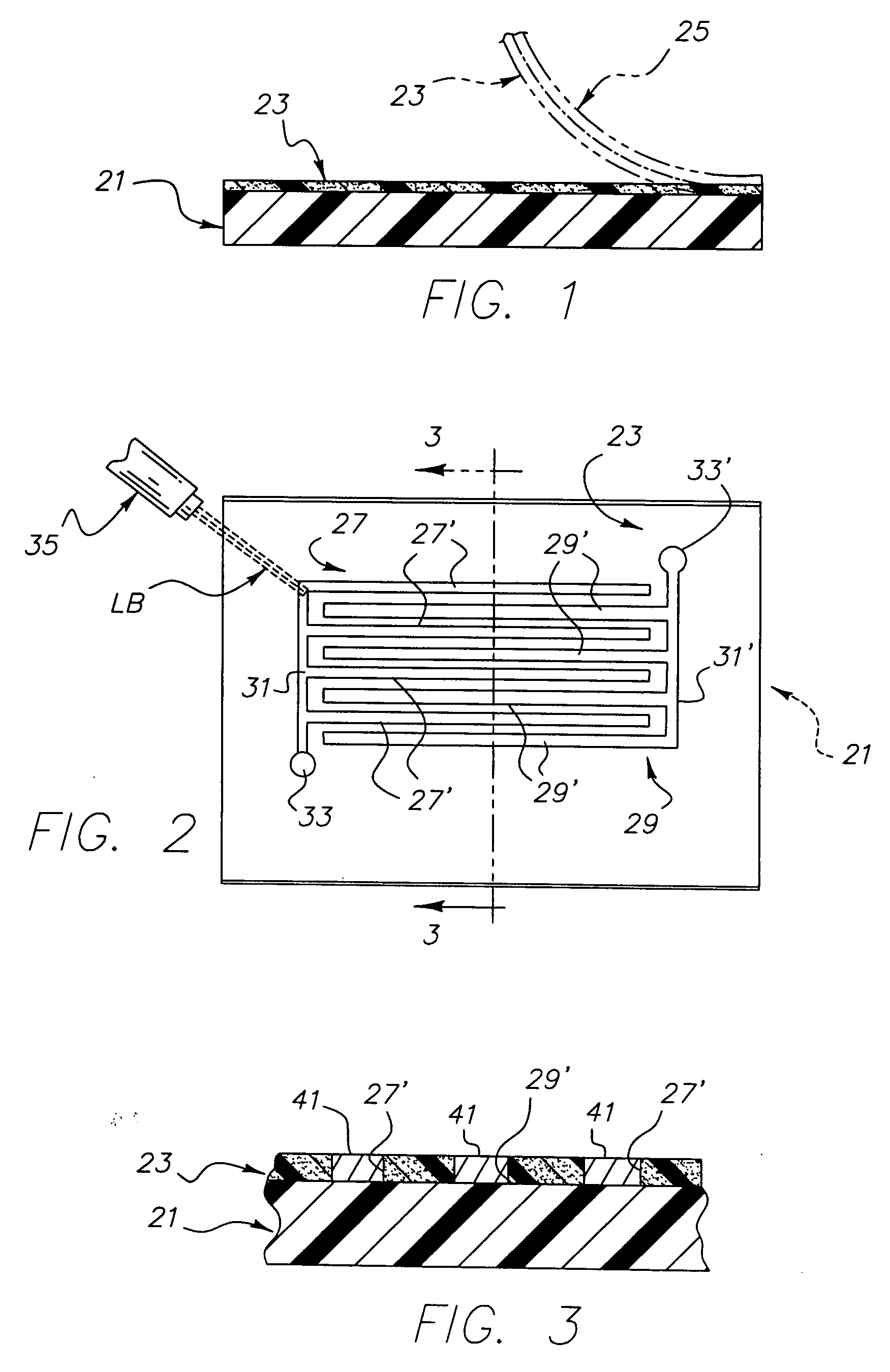
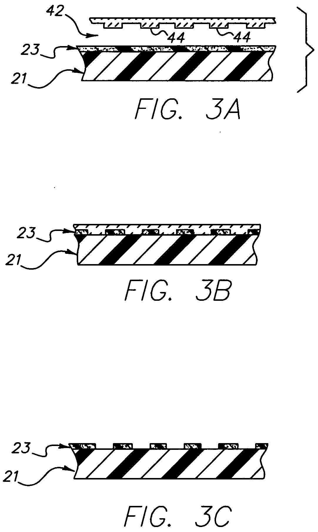
A method of making a circuitized substrate which includes at least one and possibly several capacitors as part thereof. In one embodiment, the substrate is produced by forming a layer of capacitive dielectric material on a dielectric layer and thereafter forming channels with the capacitive material, e.g., using a laser. The channels are then filled with conductive material, e.g., copper, using selected deposition techniques, e.g., sputtering, electro-less plating and electroplating. A second dielectric layer is then formed atop the capacitor and a capacitor “core” results. This “core” may then be combined with other dielectric and conductive layers to form a larger, multilayered PCB or chip carrier. In an alternative approach, the capacitive dielectric material may be photo-imageable, with the channels being formed using conventional exposure and development processing known in the art. In still another embodiment, at least two spaced-apart conductors may be formed within a metal layer deposited on a dielectric layer, these conductors defining a channel there-between. The capacitive dielectric material may then be deposited (e.g., using lamination) within the channels.

Description

TECHNICAL FIELD[0001]The present invention relates to methods of making circuitized substrates having one or more internal capacitors as part thereof.CROSS REFERENCE TO CO-PENDING APPLICATIONS[0002]In Ser. No. 11 / 031,085, entitled “Capacitor Material For Use In Circuitized Substrates, Circuitized Substrate Utilizing Same, Method of Making Said Circuitized Substrate, and Information Handling System Utilizing Said Circuitized Substrate” and filed Jan. 10, 2005, there is defined a material for use as part of an internal capacitor within a circuitized substrate wherein the material includes a polymer (e.g., a cycloaliphatic epoxy or phenoxy based) resin and a quantity of nano-powders of ferroelectric ceramic material (e.g., barium titanate) having a particle size substantially in the range of from about 0.01 microns to about 0.90 microns and a surface area for selected ones of these particles within the range of from about 2.0 to about 20 square meters per gram. A circuitized substrate ...

Claims


Application Information

Patent Timeline
IPC IPC(8): H01L21/77
CPCH01G4/206H01G4/232H01G4/33H05K1/162H05K3/0032H05K3/107H05K2201/0209H05K2201/0257H05K2201/09236H05K2201/09309H05K2201/09881H05K2203/0108H05K2203/066
Inventor DAS, RABINDRA N.EGITTO, FRANK D.LIN, HOW T.LAUFFER, JOHN M.MARKOVICH, VOYA R.
Owner ENDICOTT INTERCONNECT TECH
Why Eureka
Try Eureka