

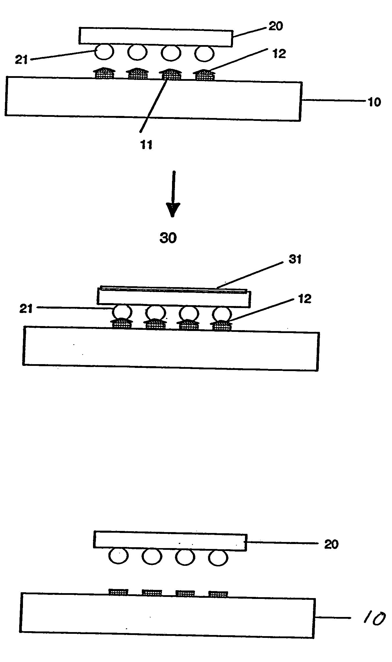
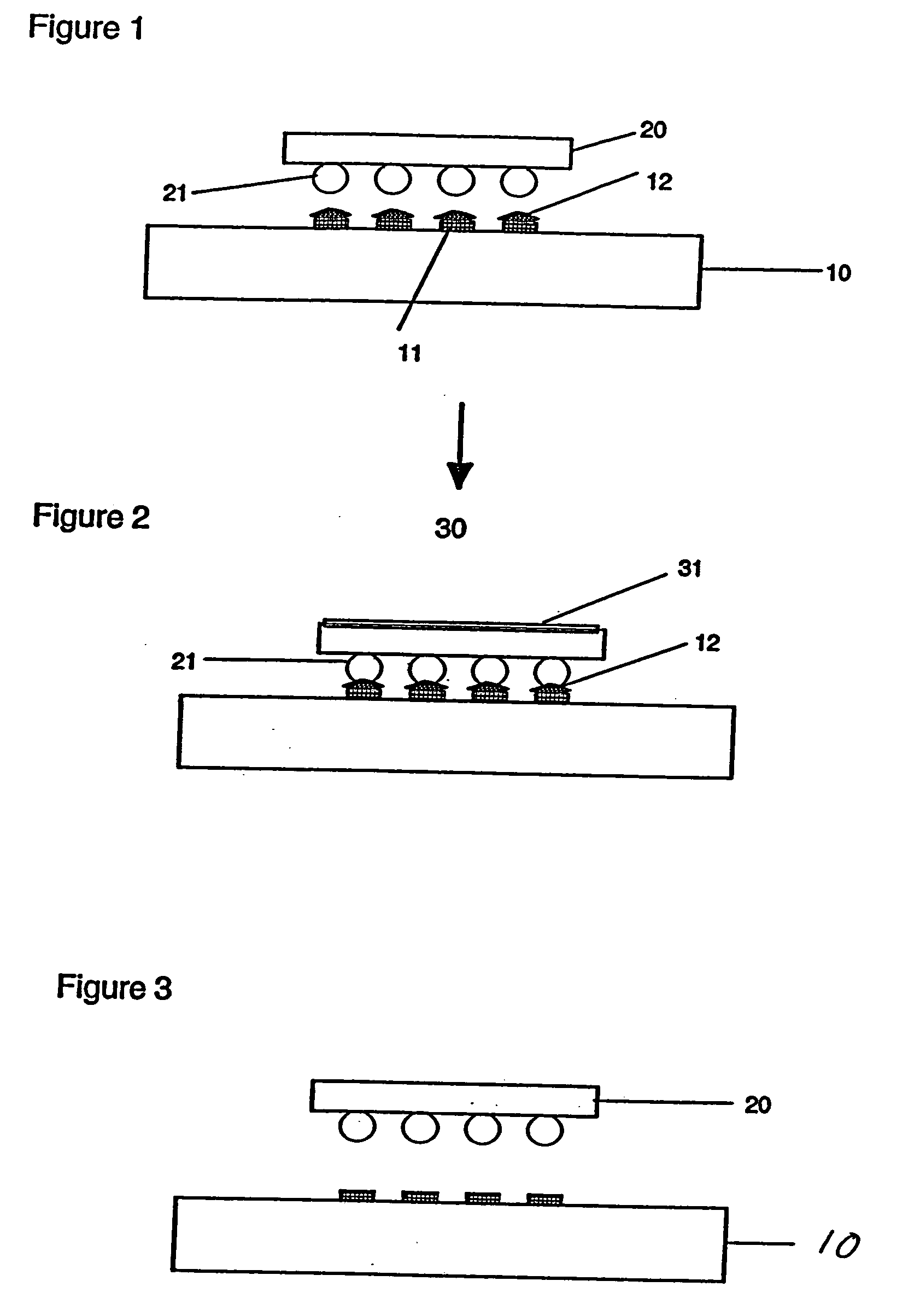
Temporary chip attach method using reworkable conductive adhesive interconnections
a technology of conductive adhesive and interconnection, which is applied in the direction of individual semiconductor device testing, semiconductor/solid-state device testing/measurement, instruments, etc., can solve the problems of affecting the chip function, limiting the applicability of this approach to alumina ceramic, and high density, and achieves the effect of maintaining pressur
- Summary
- Abstract
- Description
- Claims
- Application Information
AI Technical Summary
Benefits of technology
Problems solved by technology
Method used
Image

Examples
example 1
[0082] Dodecenylsuccinic anhydride (DDSA), 2.6 g was added to a solution of about 2.8 g of 1,3-bis(glycidoxy-propyl)tetramethyldisiloxane and 0.6 g of poly(n-butyl methacrylate) prepared by first dissolving the polymer in the liquid siloxane epoxide, and heating at 50-60° C. with stirring till a clear viscous solution was formed, then adding the anhydride and continued stirring to blend in the anhydride. The viscous mixture thus obtained was allowed to cool to room temperature and then 0.02 g of benzyldimethyl amine (BDMA), 0.03 g of 2,4,6-tris(dimethylaminomethyl) phenol (DMP-30), and 0.03 g nonylphenol were added and well mixed to form a clear homogeneous solution. About 27.5 g of Au-coated silver flake (90% Ag / 10% Au surface coated,wt % ratio) as metal filler was dispersed in the catalyzed mixture with slow addition and continued mixing to form a conductive adhesive paste having about 82 wt % filler. The paste stored at −40° C. when not in use. Relevant characterization data for ...
example 2
[0083] A mixture of Dodecenylsuccinic anhydride (DDSA), 2.6 g, 1,3-bis(glycidoxy-propyl)tetramethyldisiloxane, 2.8 g, and poly(n-butyl methacrylate),0.6 g, prepared according to the method provided in Example 1. To this mixture at room temperature was added 0.025 g of nonylphenol, 0.025 g of ethylene glycol and 0.04 g benzyldimethyl amine and well mixed till a homogeneous mixture was formed. To about 5.5 g of this final catalyzed mixture was blended in 25.5 g Au-coated Ag (90% Ag / 10% Au, wt %) filler to form a conductive adhesive paste having about 82.2% (wt %) filler loading. Measurement of resistivity and other relevant characterization data are summarized in Table 1.
example 3
[0084] To a soluble mixture of 1.55 g of a 3-bis(glycidoxypropyl)tetramethyl disiloxane, 1.1 g hexahydrophthalic anhydride (HHPA), and 0.38 g poly(acrylonitrile-co-butadiene-co-acrylic acid, dicarboxy terminated glycidyl methacrylate diester (ABGMA oligomer) was added 0.03 g nonylphenol and 0.03 g of the tertiary amine 2,4,6-tris(dimethylamino-methyl)phenol (DMP-30) and thoroughly mixed to form a clear homogeneous solution. About 12.5 g of Au-coated silver flake were blended in this catalyzed mixture to form screenable conductive adhesive paste having about 80 . . . 5 wt % of the conductive filler. Relevant characterization data are given in Table 1.
PUM
 Abstract
Description
Claims
Application Information