
Image sensor device and manufacturing method of the same

a technology of image sensor and manufacturing method, which is applied in the direction of color television, basic electric elements, television systems, etc., can solve the problems of difficult to obtain sufficient heat radiation characteristics and decrease in mounting reliability, and achieve the effects of preventing the yield or mounting reliability from being reduced, high heat radiation characteristics, and good productivity

Inactive Publication Date: 2006-09-14
PANASONIC CORP
View PDF5 Cites 10 Cited by
  • Summary
  • Abstract
  • Description
  • Claims
  • Application Information

AI Technical Summary

Benefits of technology

[0012] Accordingly, it is an object of the present invention to provide an image sensor device and a manufacturing method of the same, which is capable of preventing mounting yield or mounting reliability from being reduced and has good productivity and high heat radiation characteristics while realizing miniaturization and slimness of an electronic device.
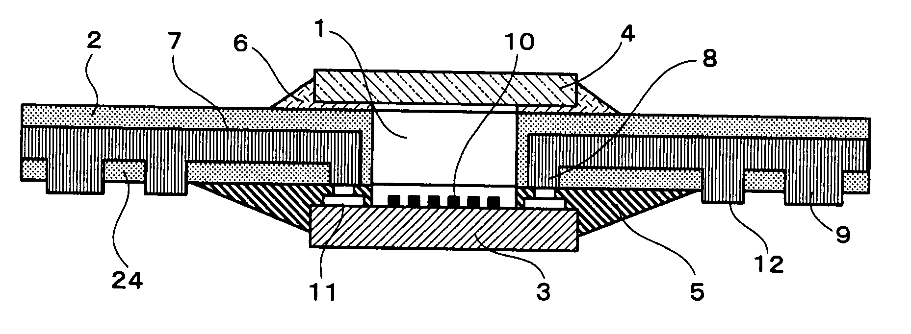
[0015] By this structure, since the metal exposing portion exposed from one surface of the base between the internal terminal portion and the external terminal portion is formed, in a case where a solder ball is not mounted on the external terminal portion, although a bled component flows from the sealing resin along one surface of the base during a manufacturing method, the bled component stops by the metal exposing portion which functions as a breakwater and thus the bled component can be prevented from covering the external terminal portion and mounting yield or mounting reliability is not reduced when the image sensor device is mounted on an electronic device. Accordingly, it is possible to suppress the image sensor device from being enlarged due to the bleed phenomenon, to easily realize the miniaturization and the slimness of the image sensor device, and to obtain good mounting yield and mounting reliability. In addition, since the metal exposing portion as well as the external terminal portion is exposed, the exposure area of the metal wiring having good heat radiation on the base increases and thus high heat radiation characteristics can be obtained. Accordingly, it is possible to obtain sufficient heat radiation characteristics in an electronic device or an image sensor which requires high heat radiation.
[0016] In addition, in the image sensor device according to the present invention, the external terminal portion and the metal exposing portion may be protruded from the one surface of the base. By this structure, a bleed phenomenon can be more prevented as compared with a case where the metal exposing portion is in the same plane as one surface of the base and it is more difficult to cover the surface of the external terminal portion with the bled component, compared with a case where the metal terminal portion is in the same plane as one surface of the base. Accordingly, it is possible to more improve the mounting reliability.
[0017] Furthermore, in the image sensor device according to the present invention, the exposure surfaces of the external terminal portion and the metal exposing portion may be substantially in the same plane. By this structure, the metal exposing portion can be more easily used as a mounting reinforcement portion of the external terminal portion, compared with a case where exposure heights of the external terminal portion and the metal exposing portion are different from each other and thus it is possible to easily improve the mounting reliability when the image sensor device is mounted on an electronic device.
[0018] Moreover, in the image sensor device according to the present invention, a connection portion for connecting the external terminal portion with the metal exposing portion in the metal wiring may be exposed from the surface of the base. By this structure, the exposure area of the metal wiring on the surface of the base more increases by the exposure area of the connection portion, compared with a case where only the external terminal portion and the metal exposing portion are exposed and it is possible to obtain higher heat radiation characteristics.
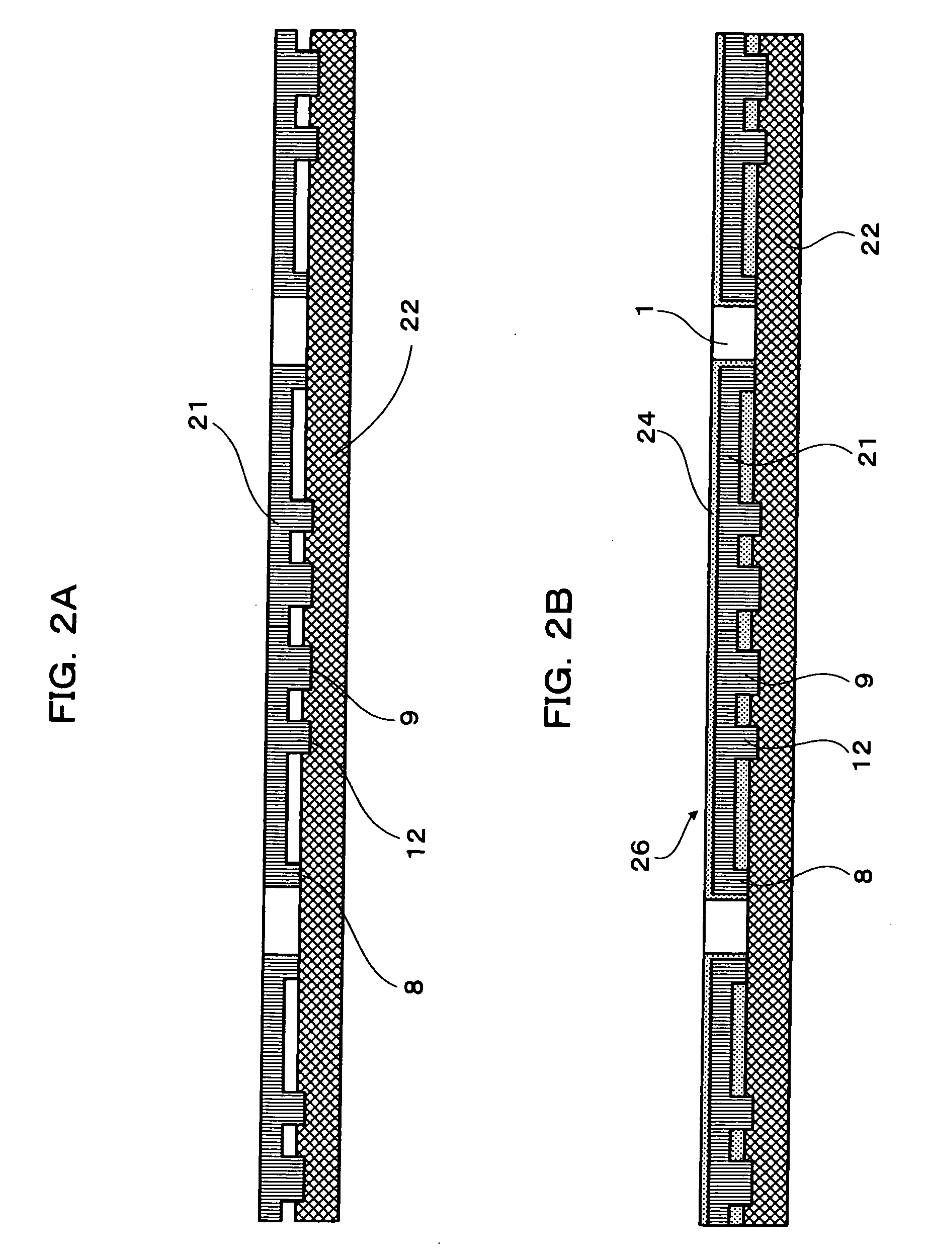
[0021] Moreover, in the method according to the present invention, the metal thin lead may be arranged so that a difference in thickness among the internal terminal portion, the external terminal portion, and the metal exposing portion in the metal wiring formed of the metal thin lead is absorbed utilizing deformation in a thickness direction of the tape material, and the sealing resin is filled in each of the cavities and cured. By this structure, it is possible to manufacture the image sensor device while absorbing the difference in the thickness between the internal terminal portion and the external terminal portion or the metal exposing portion in the metal wiring.

Problems solved by technology

Further, mounting reliability is decreased.
Accordingly, in the electronic device or the image sensor 102 which requires high heat radiation, it is difficult to obtain sufficient heat radiation characteristics.

Method used


Image

  • Image sensor device and manufacturing method of the same
  • Image sensor device and manufacturing method of the same
  • Image sensor device and manufacturing method of the same

Examples


Embodiment Construction

[0035] Hereinafter, an image sensor device and a manufacturing method of the same according to embodiments of the present invention will be described in detail with reference to the accompanying drawings.

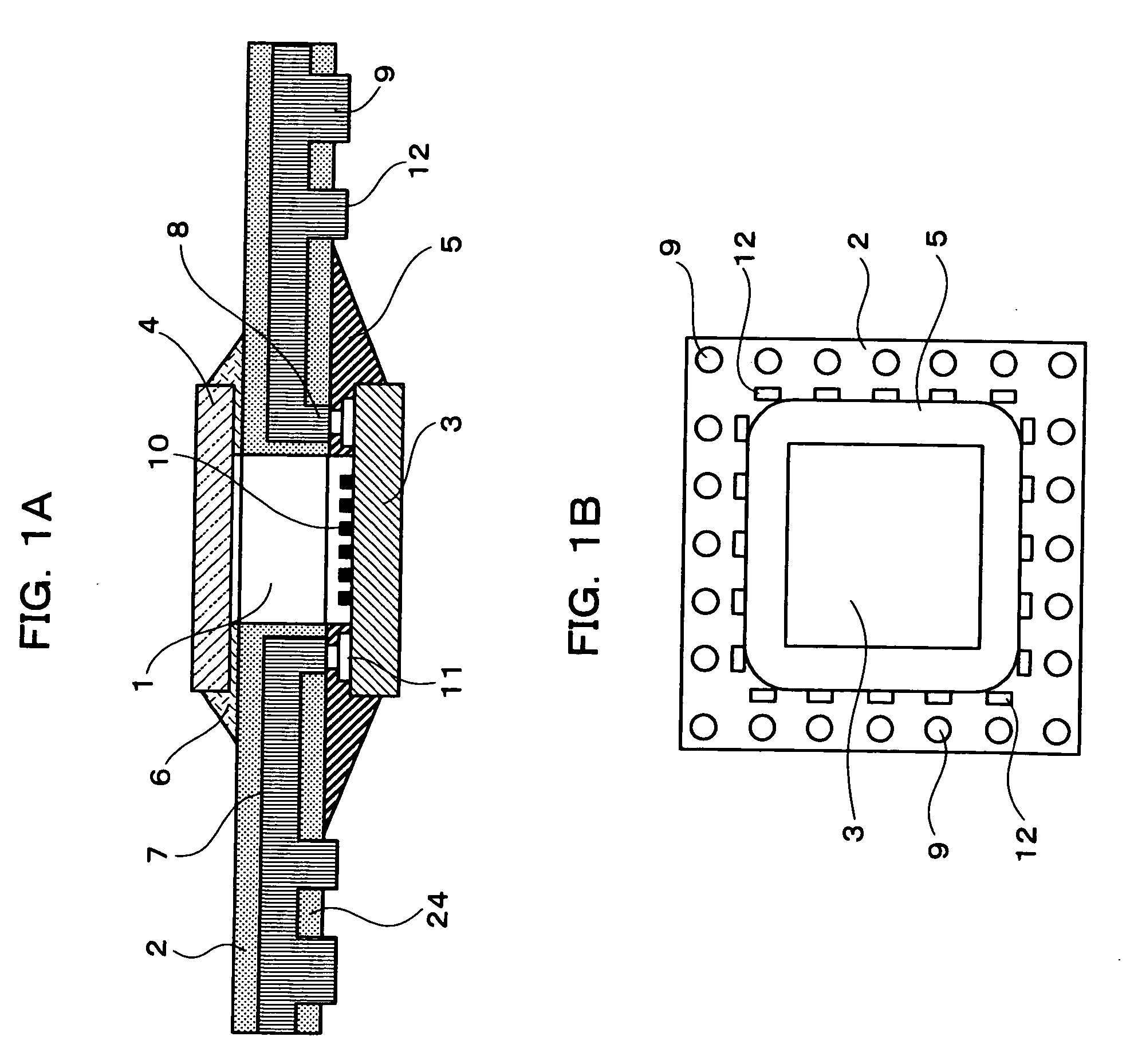
[0036] First, an image sensor device according to a first embodiment of the present invention will be described. FIG. 1A is a cross-sectional view of an image sensor device according to a first embodiment of the present invention and FIG. 1B is a bottom view of the image sensor device. In addition, in the below description, in order to facilitate understanding, a case where an image sensor is mounted on an upper surface of a base and a window member is mounted on a lower surface of the base will be described and shown. Furthermore, the window member and the image sensor need not be necessarily arranged at the upper and lower surfaces of the base, respectively, and may be positioned at any positions if the relative positions of the respective components are equal to one another.

[00...


PUM


Abstract

A metal exposing portion (12) exposed from a surface of a base (2) between an internal terminal portion (8) and an external terminal portion (9) is formed in a metal wiring (7) embedded in the base (2). Accordingly, in a case where a solder ball is not mounted on the external terminal portion (9), although a bled component flows from sealing resin along the upper surface of the base (2) during a manufacturing method, the bled component stops by the metal exposing portion (12) which function as a breakwater and thus the bled component can be prevented from covering the external terminal portion (9).

Description

BACKGROUND OF THE INVENTION [0001] 1. Field of the Invention [0002] The present invention relates to an image sensor device in which an image sensor such as a charge coupled device (CCD) is mounted on a base and a manufacturing method of the same. [0003] 2. Description of the Related Art [0004] An image sensor device is widely used in a video camera, a still camera, or a mobile phone. For example, as disclosed in Japanese Unexamined Patent Application Publication No. 2003-352082 or Japanese Unexamined Patent Application Publication No. 2002-299595, the image sensor device is provided as in a package form in which an image sensor such a charge coupled device (CCD) is mounted on a base and a light receiving region is covered by a light transmission plate. In order to miniaturize the image sensor device, the image sensor is mounted on the base in a bare chip form. This conventional image sensor device will be described with reference to FIG. 12. [0005]FIG. 12 is a cross-sectional view ...

Claims


Application Information

Patent Timeline
Patent Type & Authority Applications(United States)
IPC IPC(8): H01C7/00H01L23/02H01L23/04H01L27/14H04N25/00
CPCH01L27/14618H01L27/14683H01L31/0203H04N5/2257H01L2224/16H04N23/57
Inventor AKAHOSHI, TOSHITAKA
Owner PANASONIC CORP
Learn More