Display device

a display device and display technology, applied in static indicating devices, instruments, refuse gathering, etc., can solve the problems of increasing the likelihood of damage to the thin film transistors included in the gate driver stage and the supply of a scanning start signal (stv), and the decrease of the reliability of the display devi

Active Publication Date: 2006-09-14
SHENZHEN CHINA STAR OPTOELECTRONICS TECH CO LTD
View PDF15 Cites 25 Cited by
  • Summary
  • Abstract
  • Description
  • Claims
  • Application Information

AI Technical Summary

Benefits of technology

[0009] A motivation of the present invention is

Problems solved by technology

However, due to static electricity induced through the integrated circuits during manufacturing, reliability of the display devices is decreased.
In particu

Method used


Image

  • Display device
  • Display device
  • Display device

Examples


Embodiment Construction

[0031] The present invention will now be described more fully hereinafter with reference to the accompanying drawings, in which preferred embodiments of the invention are shown. This invention may, however, be embodied in many different forms and should not be construed as limited to the embodiments set forth herein.

[0032] In the drawings, the thickness of layers and regions are exaggerated for clarity. Like numerals refer to like elements throughout. It will be understood that when an element such as a layer, film, region, substrate, or panel is referred to as being “on” another element, it can be directly on the other element or intervening elements may also be present. In contrast, when an element is referred to as being “directly on” another element, there are no intervening elements present.

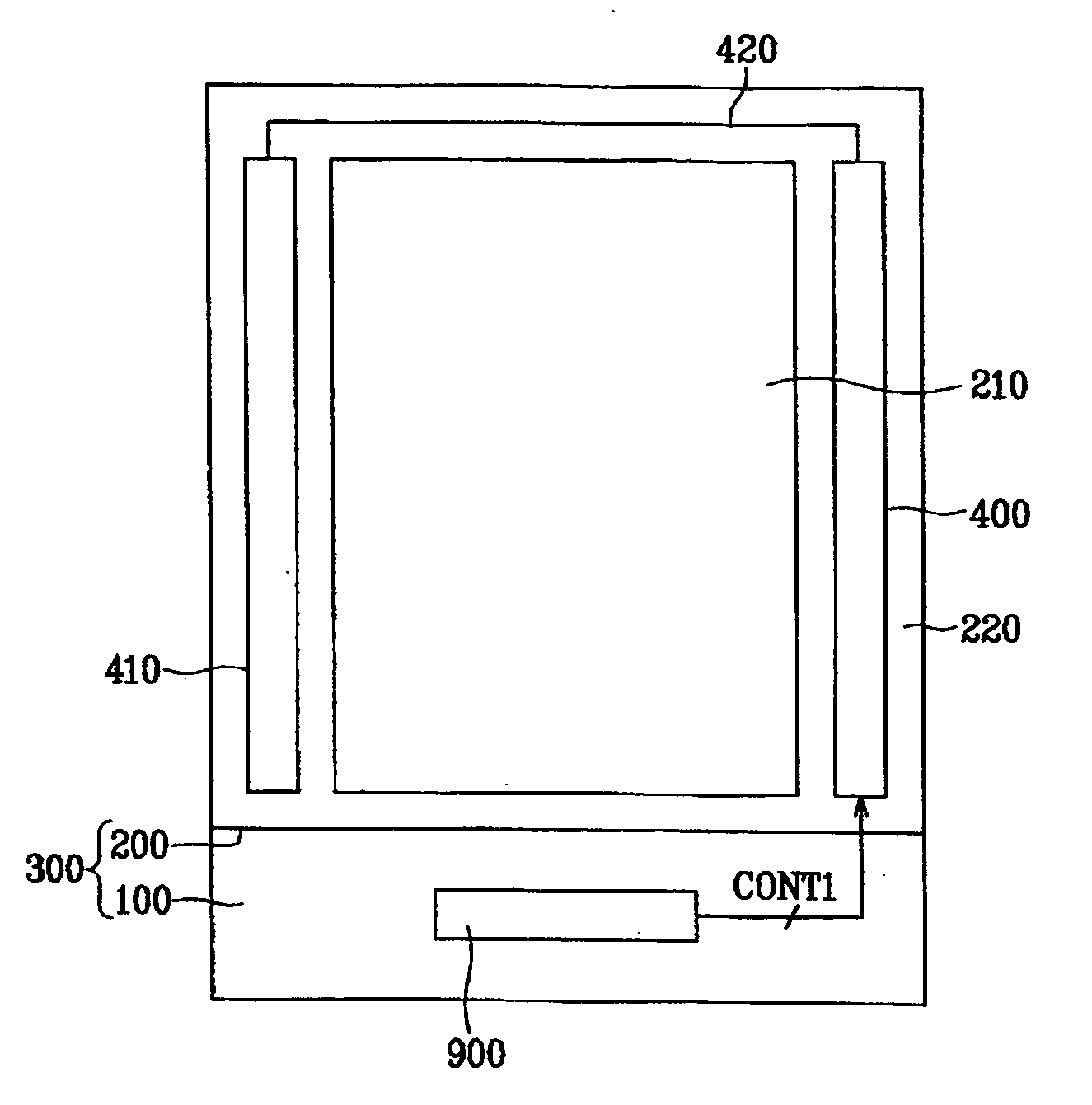
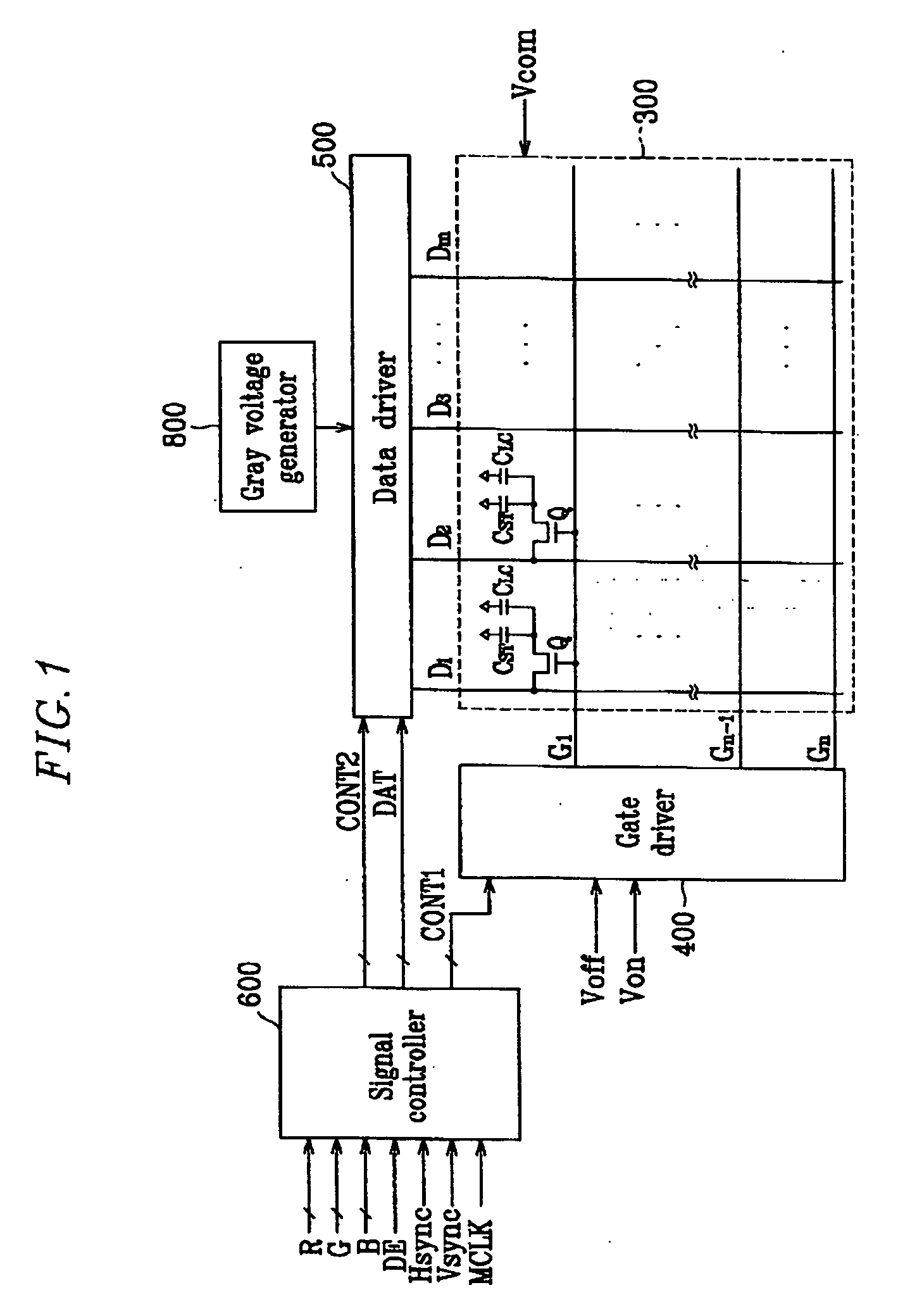
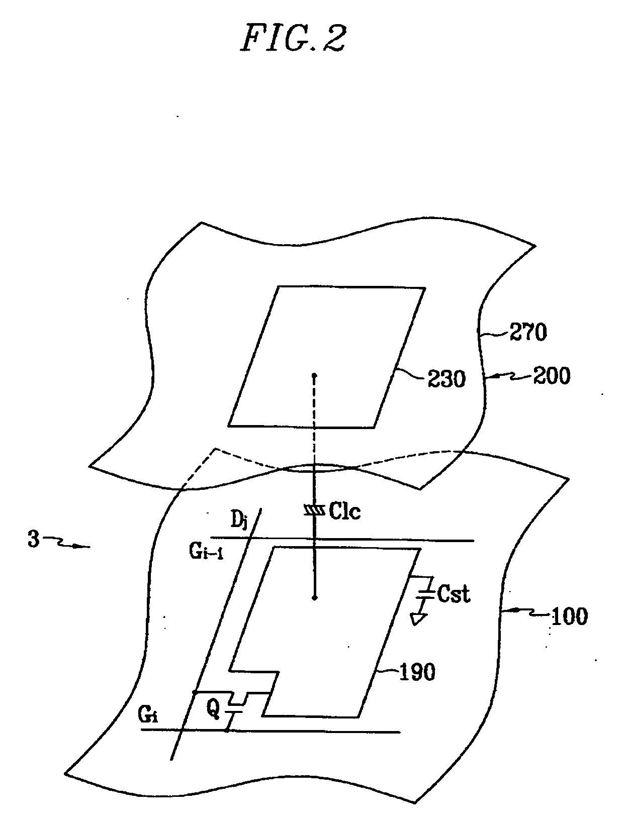
[0033]FIG. 1 is a block diagram of an LCD according to an embodiment of the present invention, and FIG. 2 is an equivalent circuit diagram of a pixel of an LCD according to an embodiment o...


PUM


Abstract

A display device is provided, which includes, a substrate, a plurality of gate lines formed on the substrate, a gate driver disposed on the substrate and transmitting gate signals to the gate lines, a repair gate driver disposed on the substrate and having a structure substantially the same as that of the gate driver, and a signal line coupled to the gate driver and the repair gate driver and transmitting at least one control signal to the gate driver.

Description

RELATED APPLICATION [0001] The present application claims priority from Korean Patent Application No. 2005-0018604, filed on Mar. 7, 2005, the disclosure of which is hereby incorporated herein by reference in its entirety. BACKGROUND [0002] (a) Field of the Invention [0003] The present invention relates to a display device. [0004] (b) Description of Related Art [0005] Display devices such as liquid crystal displays (LCDs) and organic light emitting displays (OLEDs) have a plurality of pixels arranged in a matrix format, and have switching elements selectively receiving image signals. The switching elements use elements having three terminals such as transistors. The display devices further include a plurality of gate lines, which transmit a gate-on voltage for turning on the switching elements, and a plurality of data lines which transmit image signals to the pixels coupled to the switching elements via the turned on switching elements. [0006] In addition, the display devices includ...

Claims


Application Information

Patent Timeline
IPC IPC(8): G11C8/00
CPCG02F1/13454G09G3/3648G09G3/3677G09G2300/0408G09G2330/08A47J27/002A47J27/13Y10S220/912
Inventor PARK, TAE-HYEONGKIM, CHEOL-MIN
Owner SHENZHEN CHINA STAR OPTOELECTRONICS TECH CO LTD
Why Eureka
Try Eureka