
Solid state image pickup device and camera

a solid-state image and pickup device technology, applied in the direction of radio frequency controlled devices, television system scanning details, television systems, etc., can solve the problems of color mixture with adjacent pixels, color mixture, color mixture, etc., and achieve the effect of effectively using a layou

Inactive Publication Date: 2006-09-21
CANON KK
View PDF41 Cites 116 Cited by
  • Summary
  • Abstract
  • Description
  • Claims
  • Application Information

AI Technical Summary

Benefits of technology

[0009] The invention is made in consideration of the foregoing circumstances and it is an object of the invention to provide a solid state image pickup device which can prevent color mixture by effectively using a layout of a capacitor region provided separately from a floating diffusion region and to provide a camera using such a solid state image pickup device.

Problems solved by technology

In the CMOS area sensor, however, there is a problem that a color mixture with the adjacent pixel occurs irrespective of the presence or absence of the widening function of the dynamic range mentioned above. FIGS. 8A and 8B are diagrams showing a mechanism of the occurrence of the color mixture according to conventional pixel layouts.
When the pixels having such a layout are arranged, even if a device separating region is provided between the pixels, there is a case where the color mixture cannot be avoided.
There is, consequently, such a problem that the color mixture occurs because the carriers which have been photoelectrically converted in a deep layer portion of silicon leak or light or the like which has obliquely entered and has been reflected by an aluminum layer or the like enters the adjacent photodiode.

Method used


Image

  • Solid state image pickup device and camera
  • Solid state image pickup device and camera
  • Solid state image pickup device and camera

Examples


first embodiment

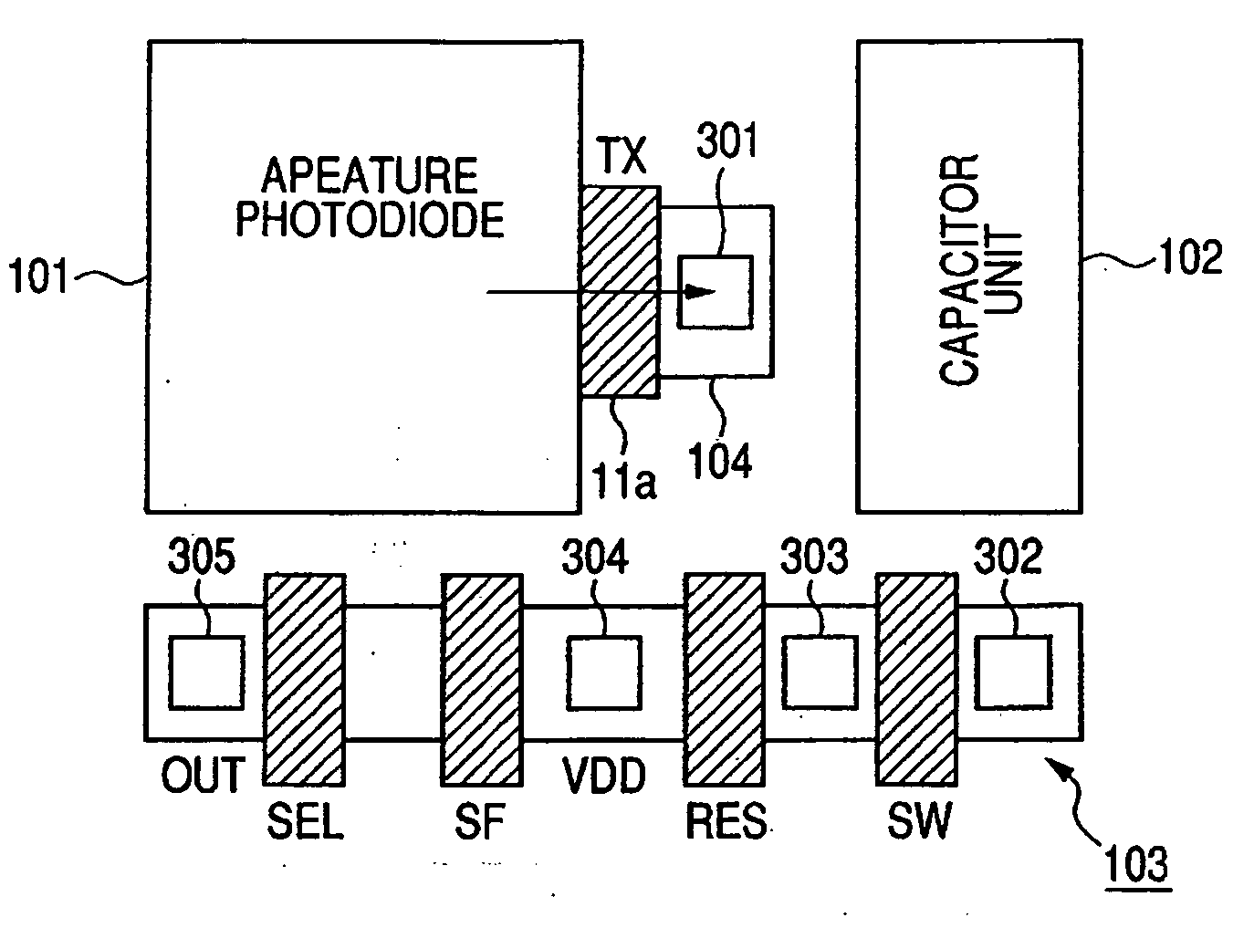
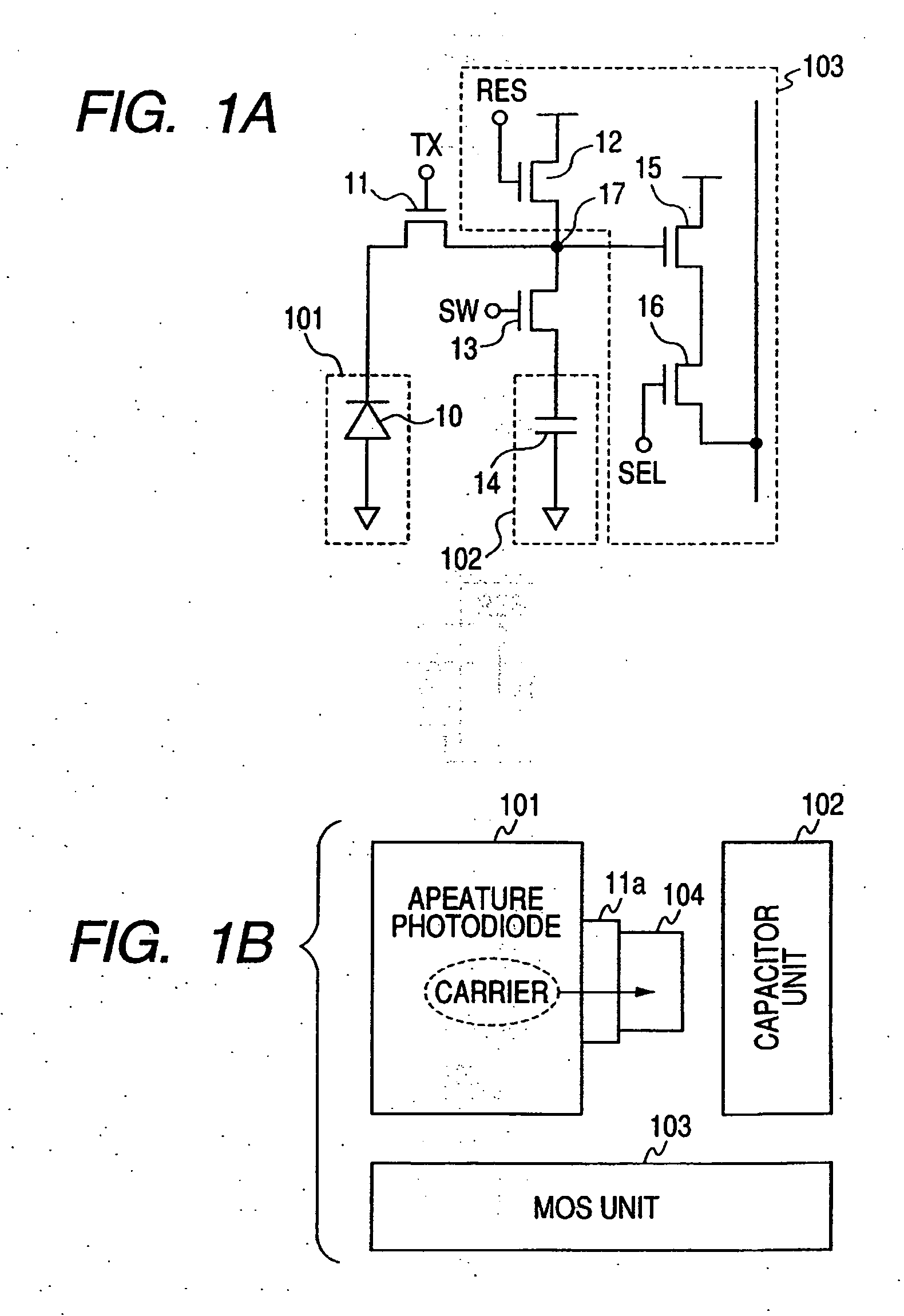
[0025] First, a solid state image pickup device (CMOS area sensor) in the first embodiment of the invention will be described. FIG. 1A is a diagram showing an example of a circuit construction of each pixel of the solid state image pickup device in the embodiment. FIG. 1B is a diagram showing a schematic example of a layout construction of each pixel of the solid state image pickup device in the embodiment.

[0026] First, the circuit construction of each pixel will be described with reference to FIG. 1A.

[0027] As shown in FIG. 1A, each pixel of the solid state image pickup device in the embodiment comprises: a photodiode 10; a first transfer MOS transistor 11; a reset MOS transistor 12; a second transfer MOS transistor 13; a carrier holding unit (capacitor) 14; a source-follower MOS transistor 15; and a selection MOS transistor 16. The pixels of the solid state image pickup device are arranged in a two-dimensional matrix shape of (a plurality of rows×a plurality of columns).

[0028] ...


PUM


Abstract

A solid state image pickup device which can prevent color mixture by using a layout of a capacitor region provided separately from a floating diffusion region and a camera using such a device are provided. A photodiode region is a rectangular region including a photodiode. A capacitor region includes a carrier holding unit and is arranged on one side of the rectangle of the photodiode region as a region having a side longer than the one side. In a MOS unit region, an output unit region including an output unit having a side longer than the other side which crosses the one side of the rectangle of the photodiode region is arranged on the other side. A gate region and the FD region are arranged between the photodiode region and the capacitor region.

Description

BACKGROUND OF THE INVENTION [0001] 1. Field of the Invention [0002] The invention relates to a solid state image pickup device and a camera and, more particularly, is suitable for use in a CMOS area sensor. [0003] 2. Related Background Art [0004] In recent years, the CMOS area sensor in which a photodiode and a MOS transistor are formed as one chip is used as a solid state image pickup device. The CMOS area sensor has such advantages that electric power consumption is smaller, a driving electric power is smaller, and a higher processing speed can be realized as compared with those of a CCD. The general CMOS area sensor is constructed by forming a plurality of pixels in a matrix shape, in which each pixel has: a photodiode; a floating diffusion (hereinbelow, also abbreviated to FD as necessary) region; a transfer transistor for transferring carriers from the photodiode to the FD region; and a reset transistor for resetting the FD region to a predetermined electric potential. [0005] A...

Claims


Application Information

Patent Timeline
Patent Type & Authority Applications(United States)
IPC IPC(8): H01L31/113H01L27/146H04N25/00
CPCH01L27/14603H01L27/14625H01L27/14645H01L27/14806H04N5/3559H04N9/045H01L27/14656H04N25/59
Inventor KOIZUMI, TORUOKITA, AKIRAOGURA, MASANORIKIKUCHI, SHINITANO, TETSUYA
Owner CANON KK
Learn More