Semiconductor circuit

Inactive Publication Date: 2006-09-21
FUJITSU MICROELECTRONICS LTD
View PDF11 Cites 0 Cited by
  • Summary
  • Abstract
  • Description
  • Claims
  • Application Information

AI Technical Summary

Benefits of technology

[0016] It is an object of the present invention to enable generation of a constant output current with a small temperature dependence, while suppressing expansion in the circuit scale but based on a circuit configuration allowing lowering in the power source voltage.
[0018] According to the present invention, it is made possible, without providing any additional voltage-current conversion circuit, to generate a constant output current with a small temperature dependence, by connecting the resistor having a positive temperature dependence so as to cancel a positive temperature dependence which resides in potential difference between base-to-emitter voltages of two transistors of the first and second transistors, as well as to suppress the circuit operation voltage to as low as 1.2 V or below because there is no need of generating a constant output voltage. It is therefore made possible to generate a constant output current with a small temperature dependence, while suppressing expansion in the circuit scale, and to lower the power source voltage.

Problems solved by technology

The circuit configured to generate a constant output voltage and to convert it into a constant output current, however, raises a difficulty in lowering the power source voltage, because elimination of the temperature dependence needs an output voltage of at least as high as approximately 1.2 V due to various physical conditions.

Method used


Image

  • Semiconductor circuit
  • Semiconductor circuit
  • Semiconductor circuit

Examples


Embodiment Construction

[0024] The following paragraphs will describe embodiments of the present invention referring to the attached drawings.

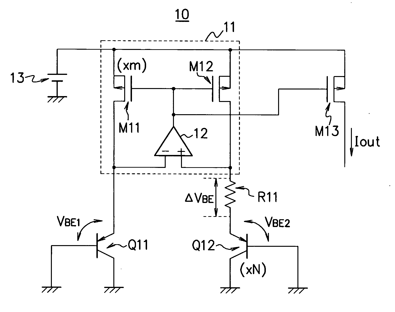
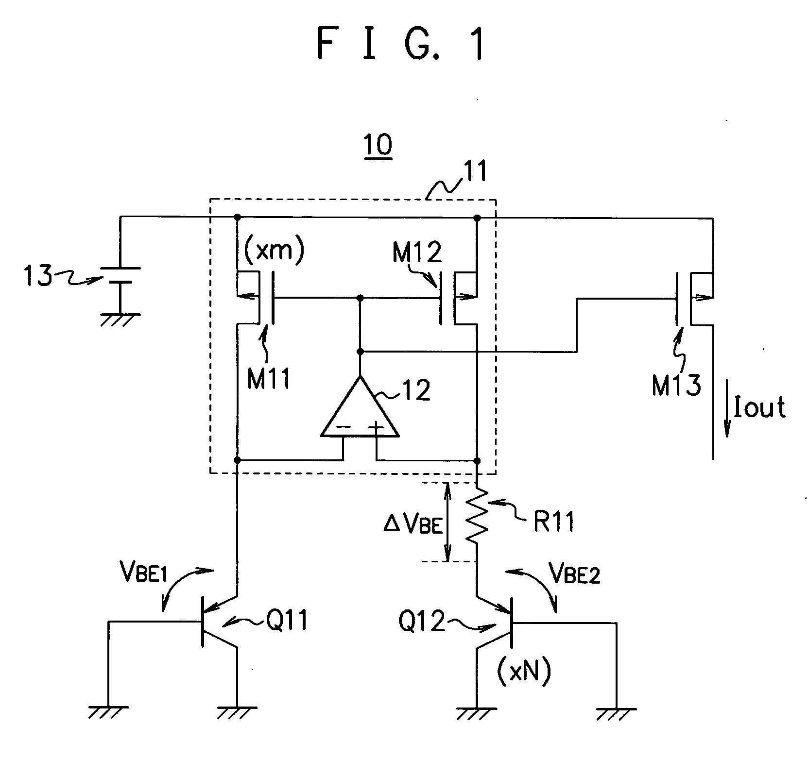
[0025]FIG. 1 is a circuit diagram showing an exemplary configuration of a reference current circuit 10 applied with the semiconductor circuit according to an embodiment of the present invention. As shown in FIG. 1, the reference current circuit 10 makes use of a band gap reference circuit, comprising pnp-type bipolar transistors Q11, Q12 respectively having both of bases and collectors thereof grounded (connected to the ground potential), a resistor R11 having one end connected in series to an emitter of the transistor Q12, and having a positive temperature dependence (temperature characteristic) with respect to the absolute temperature, an internal circuit 11 connected to an emitter of the transistor Q11 and the other end of the resistor R11, and a p-type MOS (metal oxide semiconductor) transistor M13 outputting an output current Iout corresponding to an output of ...


PUM


Abstract

A band gap reference circuit is configured by connecting an emitter of a transistor, having the base and the collector thereof grounded, to an internal circuit, and by connecting an emitter of another transistor, having the base and the collector thereof grounded, to the internal circuit via a resistor having a positive temperature dependence with respect to the absolute temperature, so as to ensure that a constant output current with a small temperature dependence can be generated, without providing any voltage-current conversion circuit and without generating a constant output voltage, while suppressing expansion in the circuit scale but based on a circuit configuration allowing lowering in the power source voltage.

Description

CROSS-REFERENCE TO RELATED APPLICATIONS [0001] This application is based upon and claims the benefit of priority from the prior Japanese Patent Application No. 2005-079947, filed on Mar. 18, 2005, the entire contents of which are incorporated herein by reference. BACKGROUND OF THE INVENTION [0002] 1. Field of the Invention [0003] The present invention relates to a semiconductor circuit generating a constant current with a small temperature dependence, preferably used as a reference current circuit or the like. [0004] 2. Description of the Related Art [0005] Conventionally, constant current output insensitive to temperature environment, or temperature-independent current output, has generally been obtained by combining a circuit called “band gap reference circuit” with a voltage-current conversion circuit. The band gap reference circuit is a reference voltage circuit capable of generating a constant output voltage without temperature dependence. A constant output current can be obtai...

Claims


Application Information

Patent Timeline
IPC IPC(8): H03K19/0175
CPCG05F3/30
Inventor MATSUDA, ATSUSHI
Owner FUJITSU MICROELECTRONICS LTD
Why Eureka
Try Eureka