
Switch control apparatus, semiconductor device test apparatus and sequence pattern generating program

a control apparatus and semiconductor technology, applied in pulse manipulation, pulse technique, instruments, etc., can solve the problems of complicated logic circuits, complicated sequence circuits, and damage to semiconductors under tes

Active Publication Date: 2006-09-21
ADVANTEST CORP
View PDF2 Cites 2 Cited by
  • Summary
  • Abstract
  • Description
  • Claims
  • Application Information

AI Technical Summary

Benefits of technology

[0015] Further, the address control module may retrieve the first open / close instruction data of the sequence pattern within a shorter time than that for the second or later open / close instruction data and stores them in both of the first and second flip-flops.

Problems solved by technology

For example, if a number of switches are open all at once, sometimes the semiconductor under test is damaged by spike voltage.
However, in case of frequently repeat of opening and closing of the switch being required, a logic circuit constituting the sequence circuit becomes complicated.
Thus, sometimes the sequence circuit becomes more complicated.

Method used


Image

  • Switch control apparatus, semiconductor device test apparatus and sequence pattern generating program
  • Switch control apparatus, semiconductor device test apparatus and sequence pattern generating program
  • Switch control apparatus, semiconductor device test apparatus and sequence pattern generating program

Examples


Embodiment Construction

[0033] The invention will now be described based on the preferred embodiments, which do not intend to limit the scope of the present invention, but exemplify the invention. All of the features and the combinations thereof described in the embodiment are not necessarily essential to the invention.

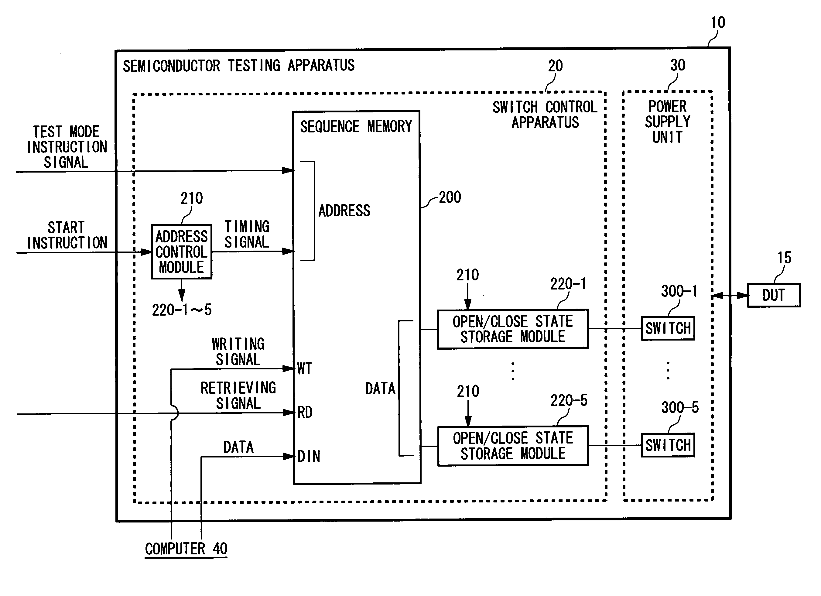
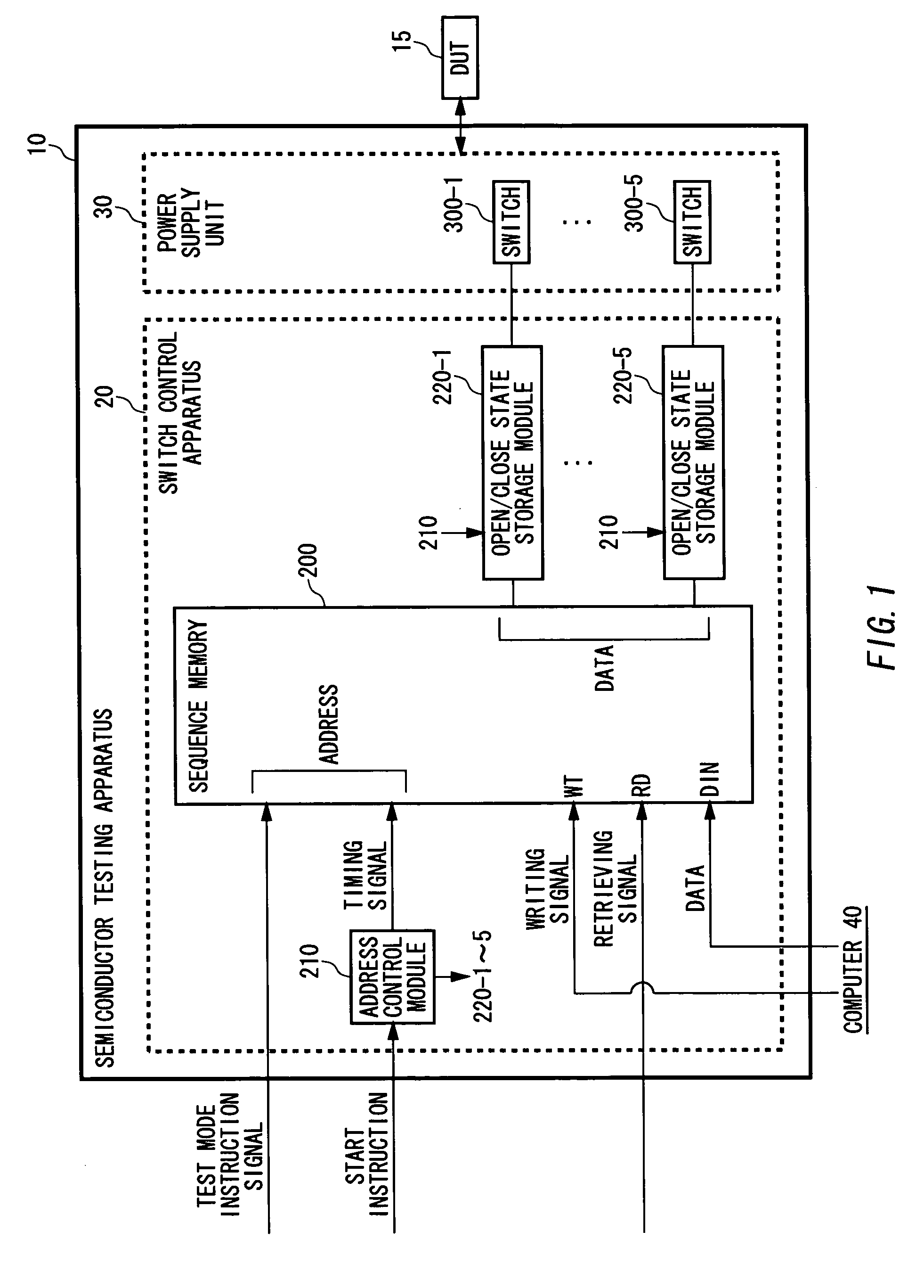
[0034]FIG. 1 is a block diagram of a semiconductor testing apparatus 10. The semiconductor testing apparatus 10 includes a switch control apparatus 20 and a power supply unit 30, controls an open / close state of a plurality of switches provided in the semiconductor testing apparatus 10, switches connection between the semiconductor testing apparatus 10 and a device under test 15 (“DUT”) to test the DUT 15. The switch control apparatus 20 includes a sequence memory 200, an address control module 210, and open / close state storage modules 220-1 to 5.

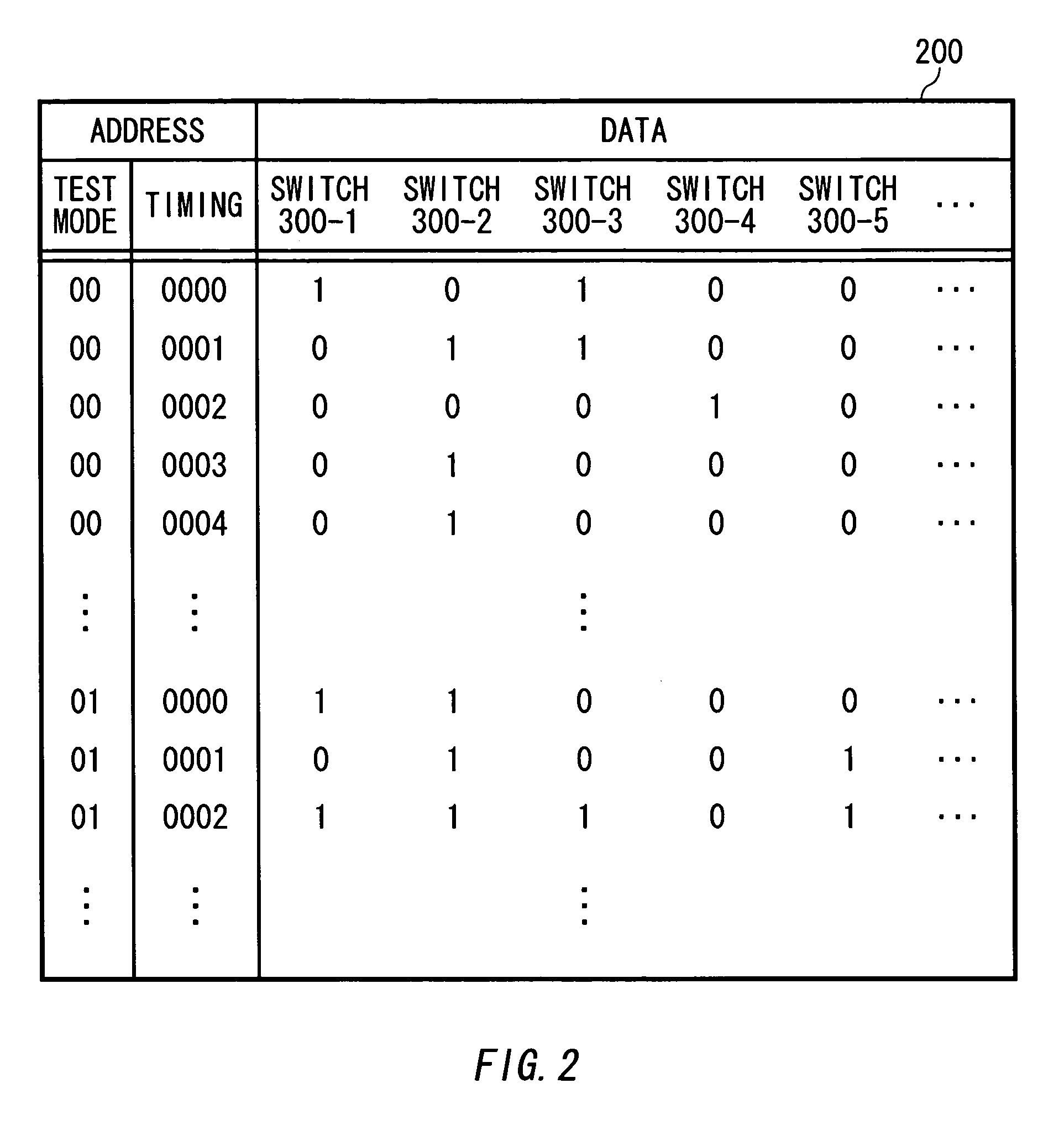
[0035] The sequence memory 200 is for example, a RAM or a ROM, on which a sequence pattern comprising open / close instruction data for instructing ...


PUM


Abstract

It is an object to properly control timing of opening and closing a switch by a circuit of simple constitution. A switch control apparatus for controlling a switch is provided, the switch control apparatus including a sequence memory for recording a sequence pattern includes open / close instruction data which instruct to open / close the switch thereon; an address control module for sequentially retrieving each of the open / close instruction data of the sequence pattern from the sequence memory; and an open / close state storage module for storing an open / close state instructed by changed open / close instruction data when the open / close instruction data retrieved by the address control module is changed, wherein the switch opens or closes in response to the open / close state stored by the open / close state storage module.

Description

[0001] This patent application claims priority from a Japanese patent application No. 2004-089022 filed on Mar. 25, 2004, the contents of which are incorporated herein by reference. BACKGROUND OF THE INVENTION [0002] 1. Field of the Invention [0003] The present invention relates to a switch control apparatus, a semiconductor testing apparatus, and a machine readable medium storing thereon a generating program. More particularly, the present invention relates to a switch control apparatus, a semiconductor testing apparatus, and a machine readable medium storing thereon a generating program for controlling timing of opening and closing a switch. [0004] 2. Description of the Related Art [0005] A number of semiconductor switches are provided in a circuit used for a semiconductor testing apparatus. Order and timing of opening and closing the switches are predetermined and if opening and closing are conducted against the order and timing, sometimes the semiconductor testing apparatus or a...

Claims


Application Information

Patent Timeline
IPC IPC(8): H03K5/19G01R31/28G01R31/3181
CPCG01R31/31813
Inventor KAWASHIMA, HIROYUKIYAMAMOTO, KAZUSHIGESHIMOYAMA, SATOSHI
Owner ADVANTEST CORP
Learn More