This helps you quickly interpret patents by identifying the three key elements:
Problems solved by technology
Method used
Benefits of technology
Benefits of technology
[0009] According to the present invention, if a predetermined wiring line which overlies a semiconducto
Problems solved by technology
However, the present inventors have found that the following problems are inherent in the IC card security technique described in this publication.
One problem with the above-described security technique is that, if the semiconductor device is operated after removing the whole of the shield layer with a chemical and if, in this state, a needle for analysis is brought into direct contact with a bus line or a signal line, it is possible to analyze information stored in the semiconductor device.
In addition, although bus lines and signal lines are covered with the multi-layer interconnection, an uncovered gap will typically occur in an input port of a module or the like in relation to the layout of the power supply wiring.
Method used
Image
Click on the blue label to locate the original text in one second.
Reading with bidirectional positioning of images and text.
Examples
first embodiment
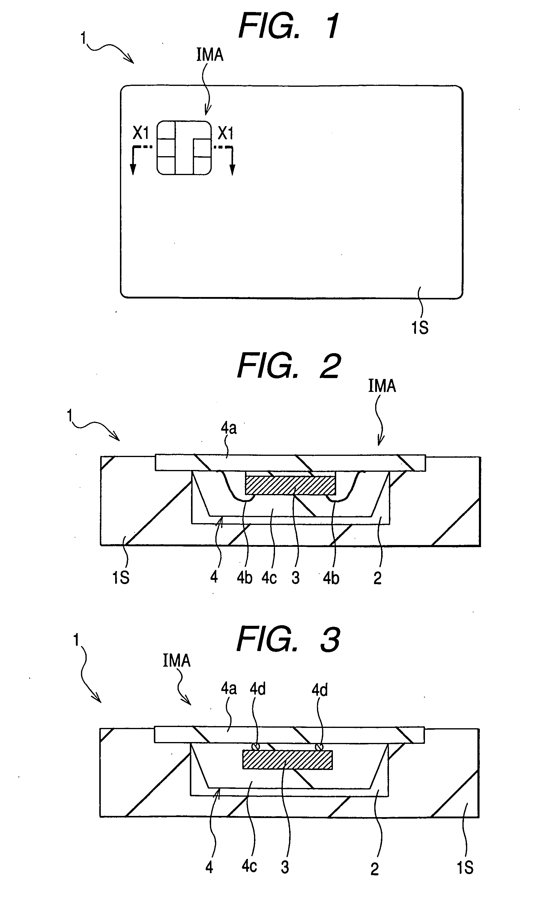
[0059]FIG. 1 is a plan view of the whole of an IC card (a semiconductor device) according to a first embodiment of the present invention, and FIG. 2 is a sectional view taken on line X1-X1 in FIG. 1.
[0060] The IC card 1 is of the type used as an information storage medium in various fields, including finance, distribution, medical care, traffic, transportation, or education, such as electronic money, credit card, portable telephone, chargeable satellite broadcast receiver, identification card, license, insurance policy, electronic medical sheet, and electronic railroad ticket. The card body 1S of the IC card 1 is constituted by a plastic sheet which is rectangular as seen in plan view, for example. The length and width of the card body 1S are, for example, 85.47 to 85.72×53.92 to 54.03 cm, and the thickness thereof is, for example, 0.68 to 1.84 mm.
[0061] In part of a main surface of the card body 1S there is provided an information storage area IMA which is generally quadrangular ...
second embodiment
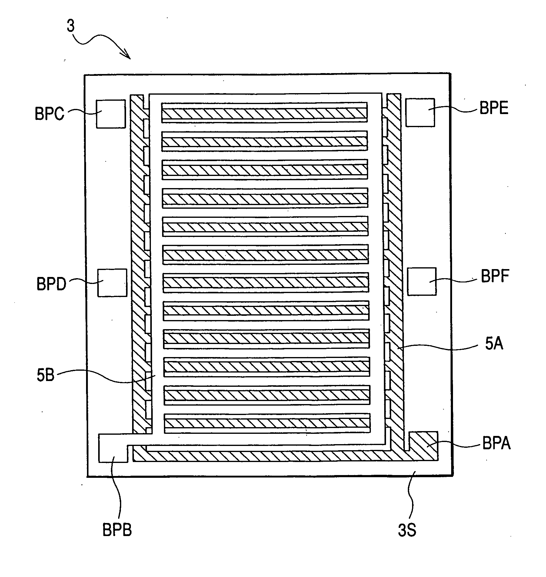
[0078]FIG. 7 is a plan view of a chip 3 which constitutes an IC card according to a second embodiment of the present invention.
[0079] In this second embodiment, as shown in FIG. 7, wiring lines 5A and 5B for the supply voltage are substantially in the shape of a ladder or grid, as seen in plan view. More specifically, the wiring lines 5A and 5B each comprise two wiring portions extending in parallel with each other vertically, as seen in FIG. 7, and plural wiring portions extending perpendicularly to the two wiring portions and arranged at predetermined intervals vertically, as seen in FIG. 7, both wiring portions being connected together at their intersecting points.
[0080] However, in this second embodiment, the wiring lines 5A and 5B are formed respectively in different wiring layers with an interlayer insulating film being disposed therebetween. In the illustrated example, the wiring line 5B for the supply voltage on a high potential side overlies the wiring line 5A for the sup...
third embodiment
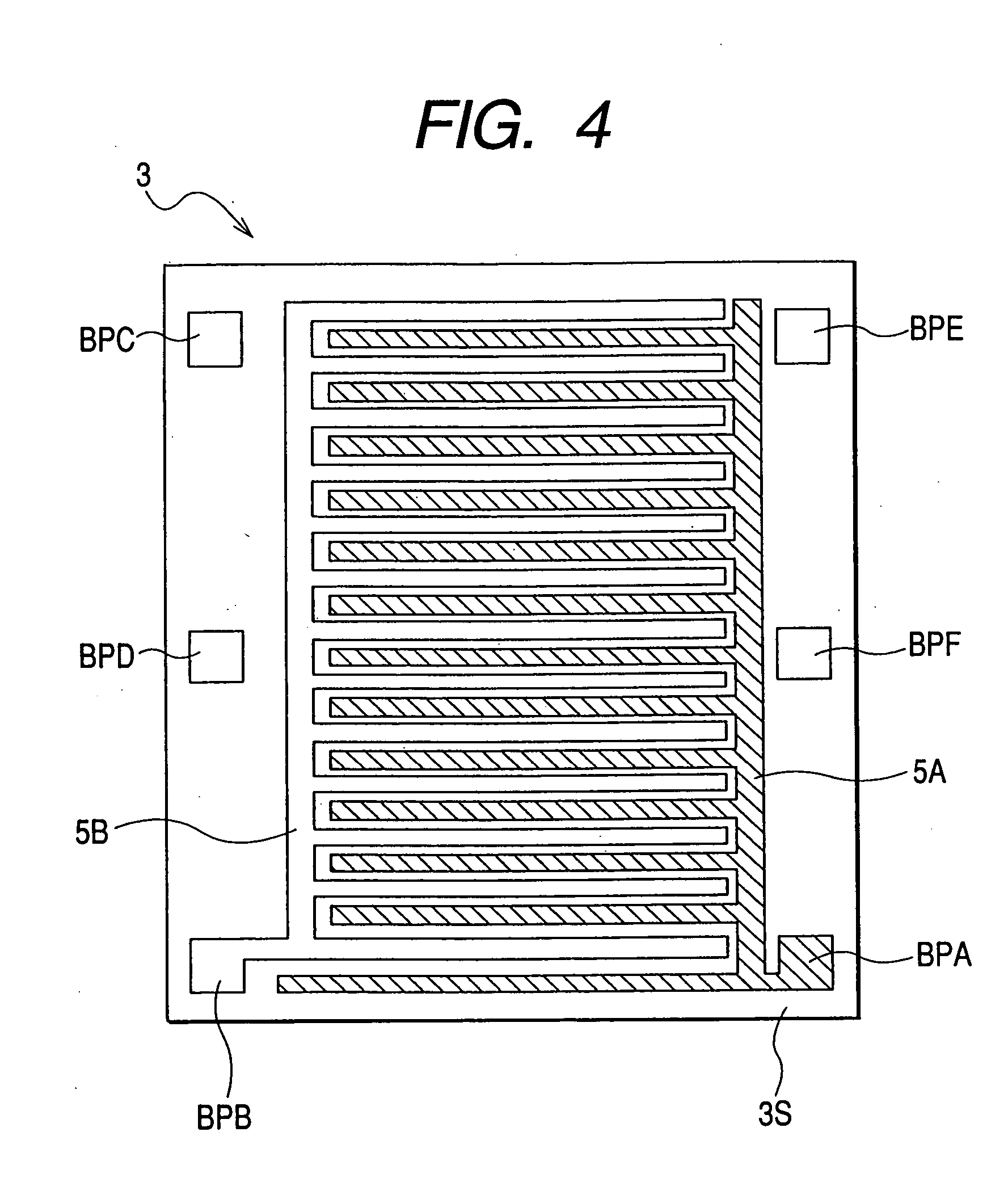
[0082]FIG. 8 is a plan view of a chip 3 which constitutes an IC card according to a third embodiment of the present invention.
[0083] In this third embodiment, as shown in FIG. 8, wiring lines 5A and 5B for the supply voltage are substantially in the shape of a lattice as seen in plan view. More specifically, the wiring lines 5A and 5B each comprise plural wiring portions extending vertically, as seen in FIG. 8, in parallel with one another and plural wiring portions extending perpendicularly thereto, both wiring portions being connected together at their intersecting points.
[0084] Also, in this third embodiment, the wiring lines 5A and 5B are formed respectively in different wiring layers. Also, in the illustrated example, the wiring lines 5B for the supply voltage on a high potential side overlie the wiring lines 5A for the supply voltage on a low potential side. Further, also in this third embodiment, the planar positions of the wiring lines 5A and 5B for the supply voltage are ...
PUM
Abstract
Wiring lines for the supply of a voltage to feed a drive voltage to an integrated circuit formed in a semiconductorchip are disposed so as to cover a main surface of the semiconductorchip, so that, if the wiring lines are removed for the purpose of analyzing information stored in the semiconductorchip, the integrated circuit does not operate and it is impossible to analyze the information. Further, there is provided a processingdetector circuit for detecting that the wiring lines have been tampered with. When the processingdetector circuit detects a change in the state of the wiring lines, the integrated circuit is reset. Thus, it is possible to improve the security of information stored on the card.
Description
CROSS-REFERENCE TO RELATED APPLICATION [0001] This application is a continuation application of application Ser. No. 10 / 486,083, filed Feb. 6, 2004, the disclosure of which is hereby incorporated by reference.TECHNICAL FIELD [0002] The present invention relates to a semiconductor device and an IC (Integrated Circuit) card technique. Particularly, the present invention is concerned with a technique which is applicable to the improvement of security for information stored in a semiconductor device. BACKGROUND OF THE INVENTION [0003] In an IC card which the present inventors have studied, the reading and writing of data from and to memory are managed by the function of a CPU (Central Processing Unit) incorporated in the IC card, and a high security function is ensured in which a cipherprocessing is executed by the card itself. Further, its memory capacity is 30 to 100 times larger than that of a magnetic card. Thus, the IC card in question is expected to see considerable use as an inf...
Claims
Application Information
Patent Timeline
Application Date:The date an application was filed.
Publication Date:The date a patent or application was officially published.
First Publication Date:The earliest publication date of a patent with the same application number.
Issue Date:Publication date of the patent grant document.
PCT Entry Date:The Entry date of PCT National Phase.
Estimated Expiry Date:The statutory expiry date of a patent right according to the Patent Law, and it is the longest term of protection that the patent right can achieve without the termination of the patent right due to other reasons(Term extension factor has been taken into account ).
Invalid Date:Actual expiry date is based on effective date or publication date of legal transaction data of invalid patent.

