Light source

a technology of light source and phosphorescent light, applied in the field of light source, can solve the problems of high panel fabrication cost and complex panel fabrication process, and achieve the effect of increasing the utilization rate of phosphorescent light emission and high-luminance light emission

Inactive Publication Date: 2006-09-28
NGK INSULATORS LTD
View PDF6 Cites 10 Cited by
  • Summary
  • Abstract
  • Description
  • Claims
  • Application Information

AI Technical Summary

Benefits of technology

[0008] It is an object of the present invention to provide a light source comprising electron emitters for increasing the rate of utilization of phosphorescent light emission based on electrons emitted from the electron emitters to achieve high-luminance light emission.

Problems solved by technology

All of these disclosed electron emitters are disadvantageous in that since no dielectric body is employed in the emitter, a forming process or a micromachining process is required between facing electrodes, a high voltage needs to be applied to emit electrons, and a panel fabrication process is complex and entails a high panel fabrication cost.

Method used


Image

  • Light source
  • Light source
  • Light source

Examples


Embodiment Construction

[0109] Light sources according to embodiments of the present invention will be described below with reference to FIGS. 1 through 63.

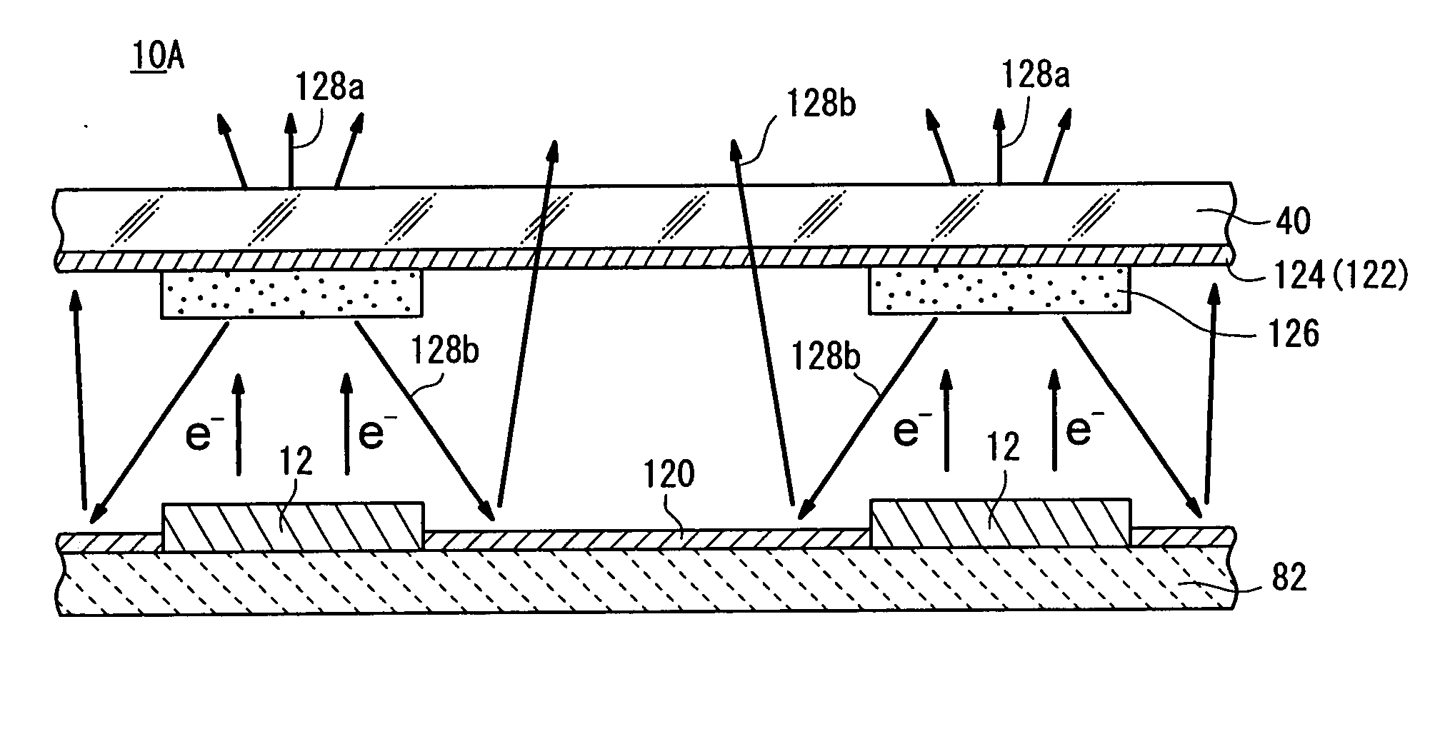
[0110] As shown in FIG. 1, a light source 10 according to an embodiment of the present invention is a light source in conformity with a display for displaying an image such as a liquid crystal display backlight or the like. As shown in FIG. 1, the light source 10 has a light emission section 14 comprising a matrix or staggered pattern of electron emitters 12 corresponding to respective light-emitting devices such as pixels, and a drive circuit 16 for driving the light emission section 14.

[0111] One electron emitter 12 may be assigned to each pixel, or a plurality of electron emitters 12 may be assigned to each pixel. In the present embodiment, it is assumed for the sake of brevity that one electron emitter 12 is assigned to each pixel.

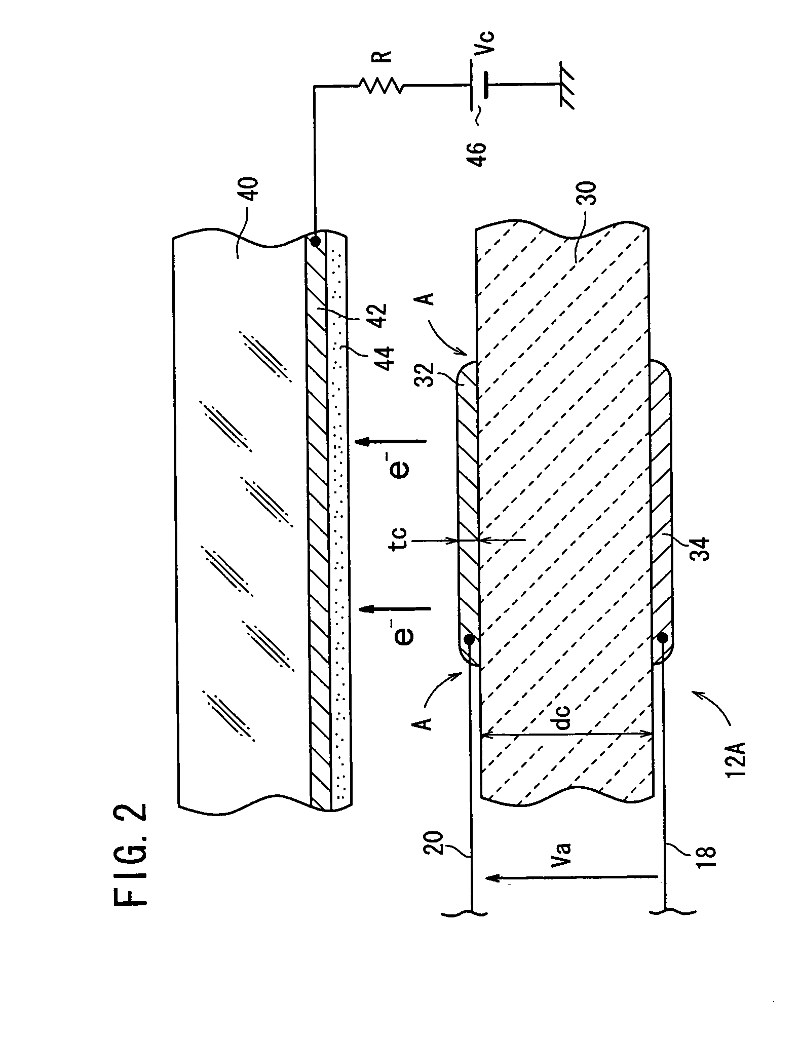
[0112] The drive circuit 16 has a plurality of row selection lines 18 for selecting rows in the light emission sectio...


PUM


Abstract

A light source has a transparent substrate, a fixed substrate disposed in facing relation to the transparent substrate, and a plurality of electron emitters disposed on a principal surface of the fixed substrate. A light reflecting film is disposed on a portion of the principal surface of the fixed substrate which is free of the electron emitters. An anode electrode in the form of a transparent electrode is disposed on a substantially entire reverse side of the transparent substrate. Phosphor layers are disposed on the anode electrode at respective positions facing the electron emitters.

Description

BACKGROUND OF THE INVENTION [0001] 1. Field of the Invention [0002] The present invention relates to a light source (including a planar light source) comprising electron emitters each for emitting electrons from an emitter by applying a drive voltage to electrodes on the emitter. [0003] 2. Description of the Related Art [0004] Recently, electron emitters having a drive electrode and a common electrode have been finding use in various applications such as field emission displays (FEDs) and backlight units. In an FED, a plurality of electron emitters are arranged in a two-dimensional array, and a plurality of phosphor layers are positioned in association with the respective electron emitters with a predetermined gap left therebetween. [0005] Conventional electron emitters are disclosed in Japanese Laid-Open Patent Publication No. 1-311533, Japanese Laid-Open Patent Publication No. 7-147131, Japanese Laid-Open Patent Publication No. 2000-285801, Japanese Patent Publication No. 46-20944...

Claims


Application Information

Patent Timeline
Patent Type & Authority Applications(United States)
IPC IPC(8): H01J63/04H01J1/62H01J61/40
CPCB82Y10/00H01J1/312H01J1/32H01J63/06H01J2201/3125H01J2329/00
Inventor OHWADA, IWAOSHIMOGAWA, NATSUMIKAMEJI, TETSUYUKIGOTO, NAOKISHIKATA, ISAO
Owner NGK INSULATORS LTD
Why Eureka
Try Eureka