Semiconductor memory device

Inactive Publication Date: 2006-09-28
KK TOSHIBA
View PDF4 Cites 49 Cited by
  • Summary
  • Abstract
  • Description
  • Claims
  • Application Information

AI Technical Summary

Problems solved by technology

Especially, it is difficult to control the written threshold levels in

Method used


Image

  • Semiconductor memory device
  • Semiconductor memory device
  • Semiconductor memory device

Examples


Embodiment Construction

[0040] Illustrative embodiments of this invention will be explained with reference to the accompanying drawings below.

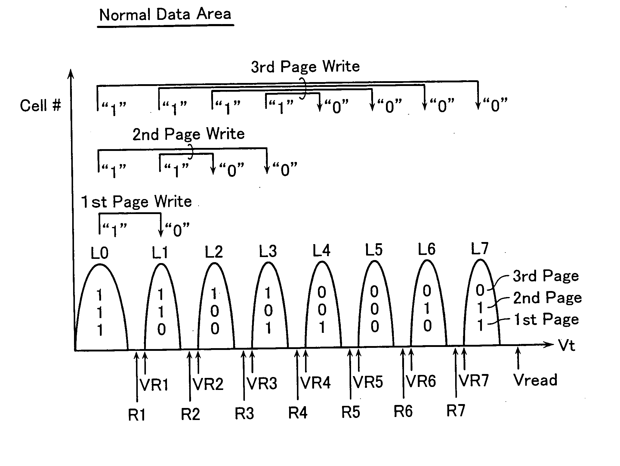
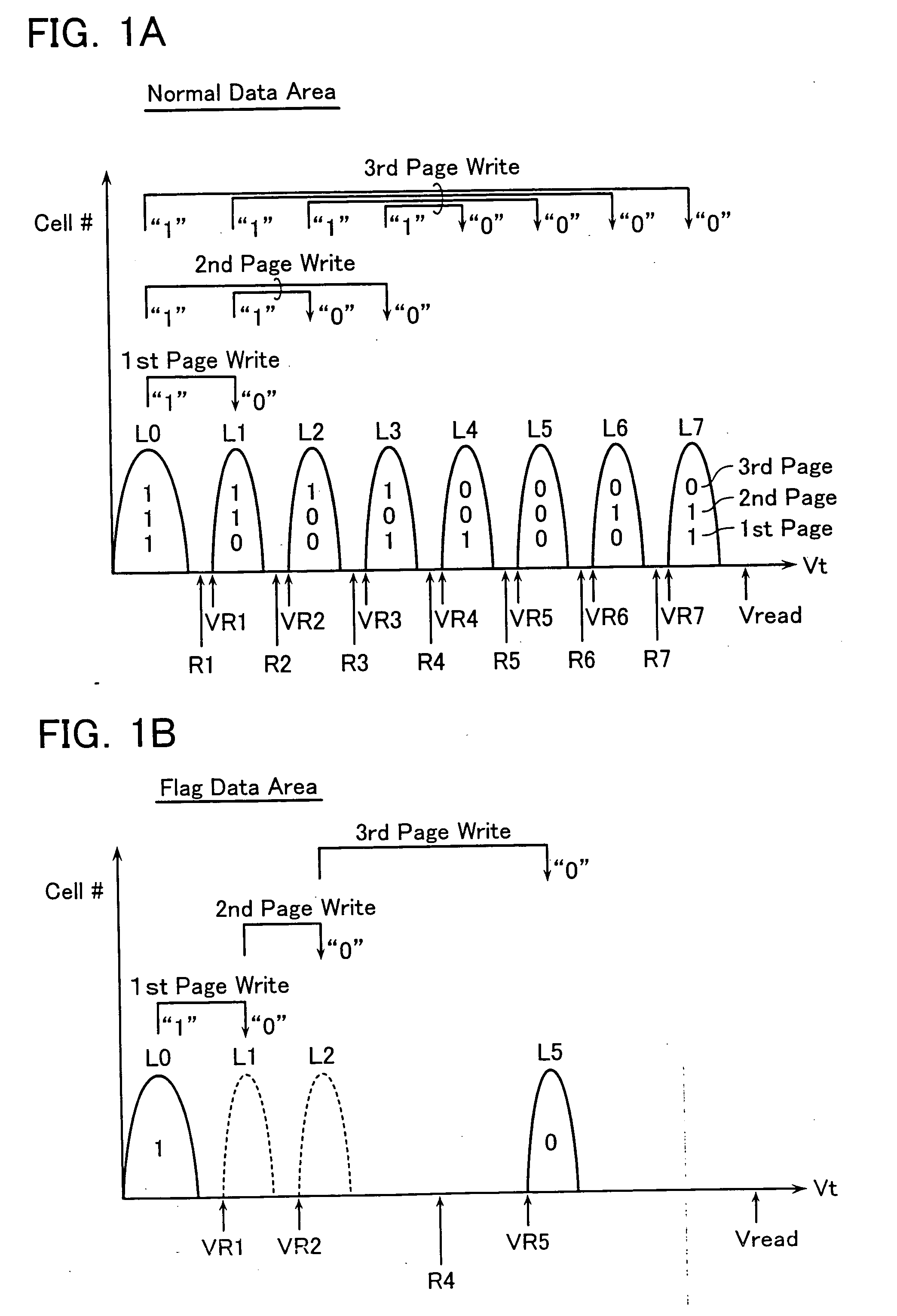
[0041] In the NAND-type flash memory in accordance with an embodiment, the memory cell array has a first area prepared for storing multi-value data (e.g., 8-value data) and a second area prepared for storing binary data. The first area is a normal data storage area while the second data area is a flag data area, which is prepared for users to be able to store some information for the normal area such as rewrite-inhibition, rewrite-limitation, rewrite-permission and the like.

[0042]FIGS. 1A and 1B show, with respect to the above-described flash memory, (a) data threshold level distributions and a bit assignment and a writing method in the normal data area for storing 8-value data, and (b) those in the flag data area which is selected or accessed simultaneously with the normal data area for storing binary data, respectively.

[0043] The entire memory cells are set in a...


PUM


Abstract

A semiconductor memory device includes a memory cell array with memory cells arranged therein, each memory cell storing data defined by threshold voltage thereof, wherein the memory cell array includes first and second areas; the first area stores multi-value data written with plural write steps; and the second area stores binary data defined by first and second logic states, threshold levels of which are controlled through the plural write steps adapted to the multi-value data write.

Description

CROSS-REFERENCE TO RELATED APPLICATION [0001] This application is based on and claims the benefit of priority from the prior Japanese Patent Application No. 2005-090855, filed on Mar. 28, 2005, the entire contents of which are incorporated herein by reference. BACKGROUND OF THE INVENTION [0002] 1. Field of the Invention [0003] This invention relates to a semiconductor memory device, especially relates to an electrically rewritable and non-volatile memory (EEPROM). [0004] 2. Description of Related Art [0005] A NAND-type flash memory is known as one of EEPROMs. In the NAND-type flash memory, a memory cell array is formed of NAND cell units with a small unit cell area, in which plural memory cells are connected in series to constitute a NAND cell unit. Therefore, the memory capacitance may be easily increased in comparison with a NOR-type flash memory. [0006] Recently, to achieve a large capacitive NAND-type flash memory, there have been provided various kinds of multi-value storage sc...

Claims


Application Information

Patent Timeline
IPC IPC(8): G11C11/34G11C16/04
CPCG11C11/5628G11C16/0483G11C16/10G11C2211/5621G11C2211/5641G11C2211/5646
Inventor HONMA, MITSUAKISHIBATA, NOBORUKANEBAKO, KAZUNORI
Owner KK TOSHIBA
Why Eureka
Try Eureka