Nonvolatile semiconductor memory device

a semiconductor and memory device technology, applied in static storage, digital storage, instruments, etc., can solve the problem of taking time to transfer write data, and achieve the effect of reducing the number of data transfers, and speeding up the write operation

Inactive Publication Date: 2005-05-19
RENESAS ELECTRONICS CORP
View PDF5 Cites 47 Cited by
  • Summary
  • Abstract
  • Description
  • Claims
  • Application Information

AI Technical Summary

Benefits of technology

[0015] (1) The nonvolatile semiconductor memory device has a write mode in which, out of a plurality of threshold voltage distributions, write operation is performed from the side of a lower threshold voltage distribution; write processing for each threshold voltage distribution out of the plurality of threshold voltage distributions is applied to memory cells to be written in; and upper limit determination processing to confirm that no excessive writing of each threshold voltage distribution is performed without discriminating any of the memory cells from others. This write mode contributes to reducing, in a configuration having a sense latch circuit connected to each memory cell and memory circuits (SRAMs) connected to this sense latch circuit via a common input / output line, the number of data transfers from the SRAMs to the sense latch circuit. In the implementation of this mode, write processing and upper limit determination processing are consecutively performed for each threshold voltage distribution.
[0017] (3) In (2) above, upper limit determination processing is to determine the memory cell subject to upper limit determination on the basis of data stored in the memory cell, and to perform additional write processing for writing again, without erasure, into any memory cell on a word line having already undergone write processing. It is thereby made possible to write again without performing erase processing.
[0018] Thus the nonvolatile semiconductor memory device according to the invention embodies a technique to form, in a memory array configuration comprising multi-value memory cells, threshold voltage distributions from the lower side upward and to thereby accelerate write verify determination. By forming threshold voltage distributions from the lower side upward, where all the memory cells in the threshold voltage distributions have surpassed the lower limit of these threshold voltage distributions, verify determination is performed only to confirm that there is no memory cell having a threshold voltage above the upper limit of these threshold voltage distributions, and accordingly it is made possible to eliminate the need for consideration of memory cells in other already formed threshold voltage distributions. Thus this technique enables write operation to be increased in speed.
[0019] Therefore, as stated above, the write mode in which threshold voltage distributions of multi-value memory cells are written from the lower voltage side in Y access circuits of the 1×sense latch circuit+2×SRAM configuration is used, and it is thereby made possible to reduce the number of data transfers from the SRAMs to the sense latch circuit and thereby to increase the speed of write operation.
[0020] It is further made possible also to reduce the number of data transfers from the SRAMs to the sense latch circuit and thereby to increase the speed of write operation by adopting a write mode in which upper limit determination is used. Furthermore, as the use of upper limit determination makes possible additional writing, no erasure is needed when memory cells on one word line are to be divided a plurality of times and written in, and this also contributes to shortening the length of writing time.

Problems solved by technology

The aforementioned 1×sense latch circuit+2×SRAM configuration, unlike the 1×sense latch circuit+2×data latch circuit configuration, involves a problem that it takes time to transfer write data on the SRAMs to the sense latch circuit.

Method used


Image

  • Nonvolatile semiconductor memory device
  • Nonvolatile semiconductor memory device
  • Nonvolatile semiconductor memory device

Examples


Embodiment Construction

[0052] The best modes for carrying out the present invention will be described in detail below with reference to drawings. In all the drawings illustrating the modes for implementation, members having the same function will be denoted by respectively the same reference signs, and their description will not be repeated.

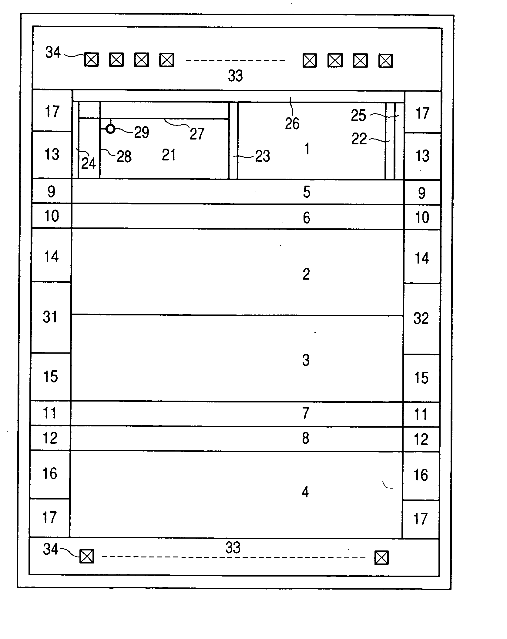
[0053] One example of configuration of a flash memory in one mode of realizing the nonvolatile semiconductor memory device will be described with reference to FIG. 1.

[0054] The flash memory in this mode for carrying out the invention maybe for example, though not limited to, a flash memory configured of a plurality of banks capable of storing in each of its memory cells data of a plurality of bits as a threshold voltage and each capable of operating independently of others; it comprises four banks 1 through 4; sense latch rows 5 through 8, Y access circuits 9 through 12 and SRAMs 13 through 16 respectively corresponding to the banks 1 through 4; and an indirect circu...


PUM


Abstract

This is a nonvolatile semiconductor memory device capable of raising the speed of write operation of Y access circuits in a 1×sense latch circuit+2×SRAM configuration. In a multi-value flash memory, in a mode of writing from the lower voltage side, writing and erratic determination are performed after data are transferred from SRAMs to a sense latch circuit for “10” and “00” distributions; after the data transfer for “01” distribution, writing is done; after the data transfer for “11” distribution word disturb determination is done; and simplified upper limit determination is done in this sequence. In particular by (1) writing from the lower voltage side of the threshold voltage distribution in the multi-value memory and (2) consecutive application of “write processing” and “upper limit determination processing” to each threshold voltage distribution, after the end of write processing for “10” and “00” distribution, since the threshold voltages of all the memory cells are lower than the upper limit determination voltages of the “10” and “00” distributions, no transfer of write data is needed in upper limit determination processing because other threshold voltage distributions are not masked.

Description

BACKGROUND OF THE INVENTION [0001] 1. Technical Field [0002] The present invention relates to a semiconductor memory device, and more particularly to a technique that can be effectively applied to the write operation of a nonvolatile semiconductor memory device, such as a multi-value flash memory having a memory array so configured that each of a plurality of memory cells can store data of a plurality of bits as a threshold voltage in Y access circuits each of a 1×sense latch circuit+2×SRAM configuration. [0003] 2. Background Art [0004] According to the findings of research by the present inventor, the following techniques are conceivable for application to a flash memory as an example of nonvolatile semiconductor memory device. [0005] For instance, a flash memory uses nonvolatile memory elements each having a control gate and a floating gate as memory cells, and each memory cell can be configured of one transistor. For such a flash memory, with a view to increasing the storage capa...

Claims


Application Information

Patent Timeline
Patent Type & Authority Applications(United States)
IPC IPC(8): G11C11/00G11C11/56G11C16/24G11C16/26
CPCG11C11/5628G11C16/26G11C16/24G11C11/5642
Inventor TAKASE, YOSHINORIKURATA, HIDEAKIYOSHIDA, KEIICHIKANAMITSU, MICHITARO
Owner RENESAS ELECTRONICS CORP
Why Eureka
Try Eureka