Semiconductor memory device

a memory device and semiconductor technology, applied in the field of semiconductor memory devices, can solve the problems of increasing cost, affecting the actual product, and extending the permissible range of capacitance variance,

Inactive Publication Date: 2001-06-12
NEC ELECTRONICS CORP
View PDF4 Cites 49 Cited by
  • Summary
  • Abstract
  • Description
  • Claims
  • Application Information

AI Technical Summary

Problems solved by technology

However, when the capacitor is realized by such a serial connection, a large area is required, and this in turn causes an increase in cost.
However, because the properties of the variance in gate capacitance and the properties of the variance in memory cell capacitance differ from each other, in a method that realizes this capacitor using gate capacitance, the variance of capacitance exceeds the permissible range, and there are problems in really applying this to actual products.
In addition to the problem of this variance in capacitance, there is the problem that the variance in the capacitance of this feedback capacitor influences the yield.
Furthermore, in comparison to the main sense amplifier, because feedback capacitors must be respectively provided for a plurality of sub-sense amplifiers, the above-described problem becomes severe.
In the above-described second example of conventional art, there is the problem that the yield is low because the variance of the threshold of the memory cells, which are much more numerous than SSAs, influences the operational margin.

Method used


Image

  • Semiconductor memory device
  • Semiconductor memory device
  • Semiconductor memory device

Examples


first embodiment

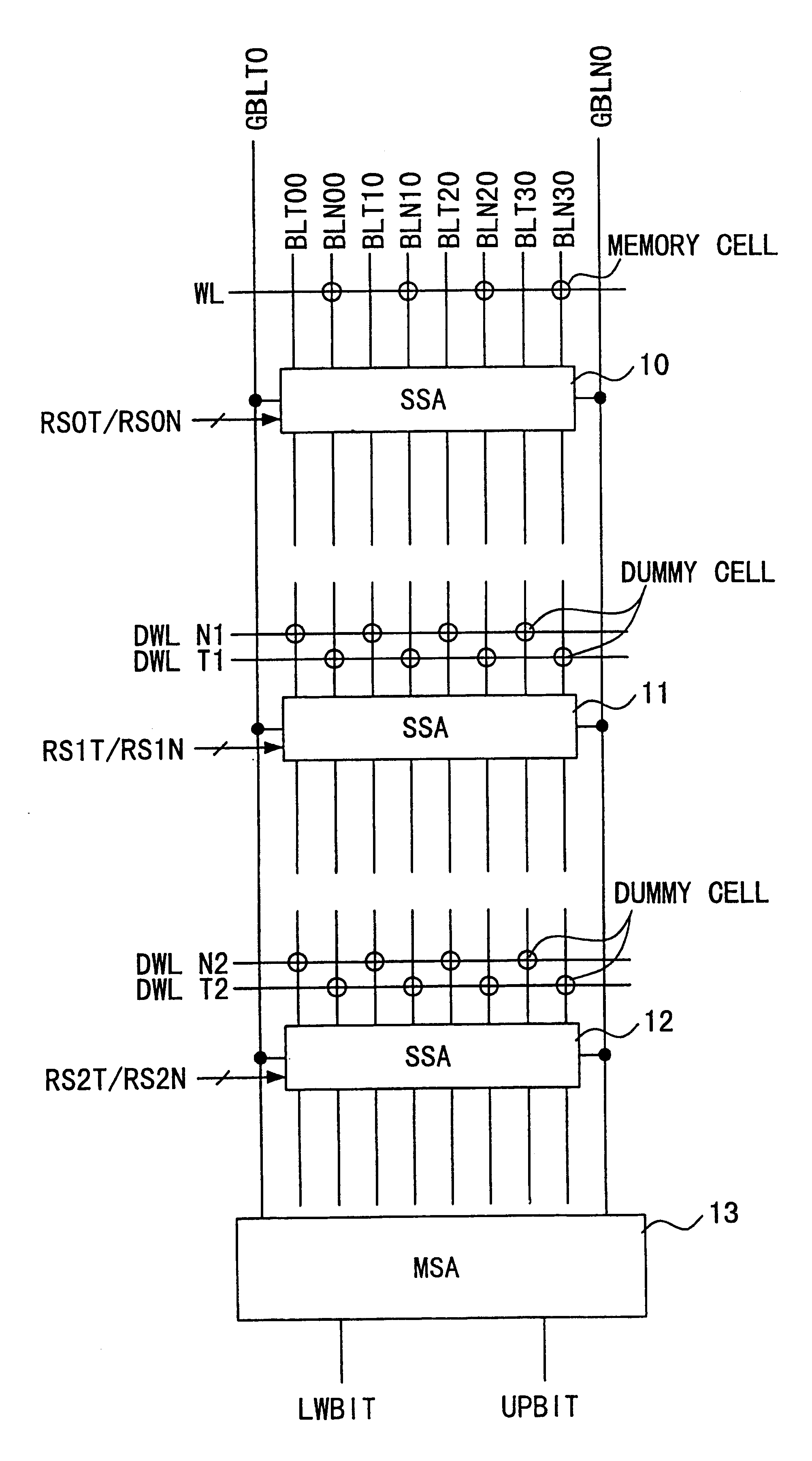
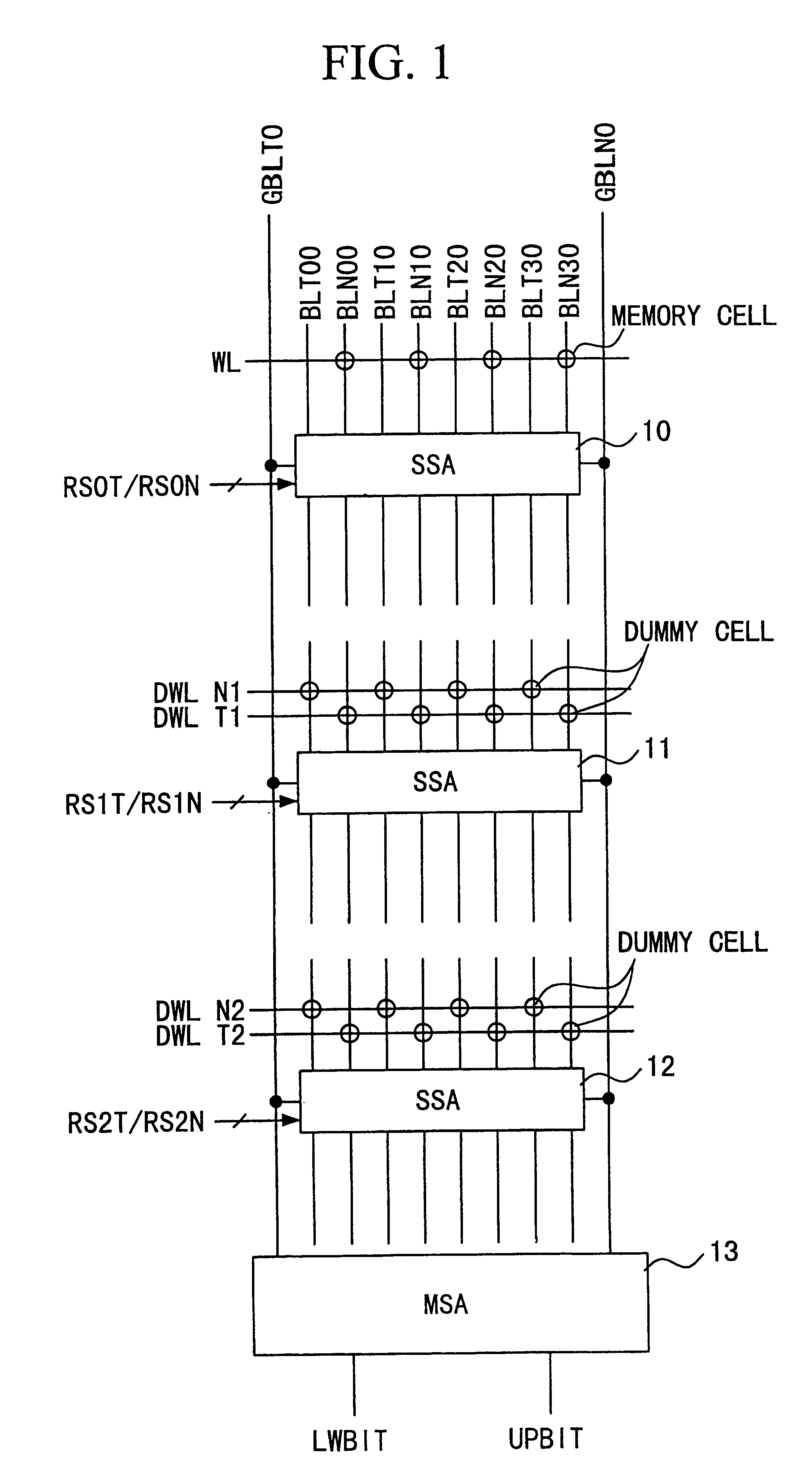
FIG. 1 is a block diagram showing the structure of the essential elements of a DRAM according to the first embodiment, and like the first example of conventional art, is drawn by extracting only the parts related to the memory cell and sense amplifiers. For circuits other than those illustrated, circuits having the same functions as a circuits provided with a typical multi-value DRAM can be used. In addition, the memory cell array of the DRAM is formed by being partitioned into a plurality of sub-arrays, and in this figure, among the plurality of sub-arrays, only the three sub-arrays activated when carrying out the reading / writing of the memory cells included in specific sub-arrays are shown.

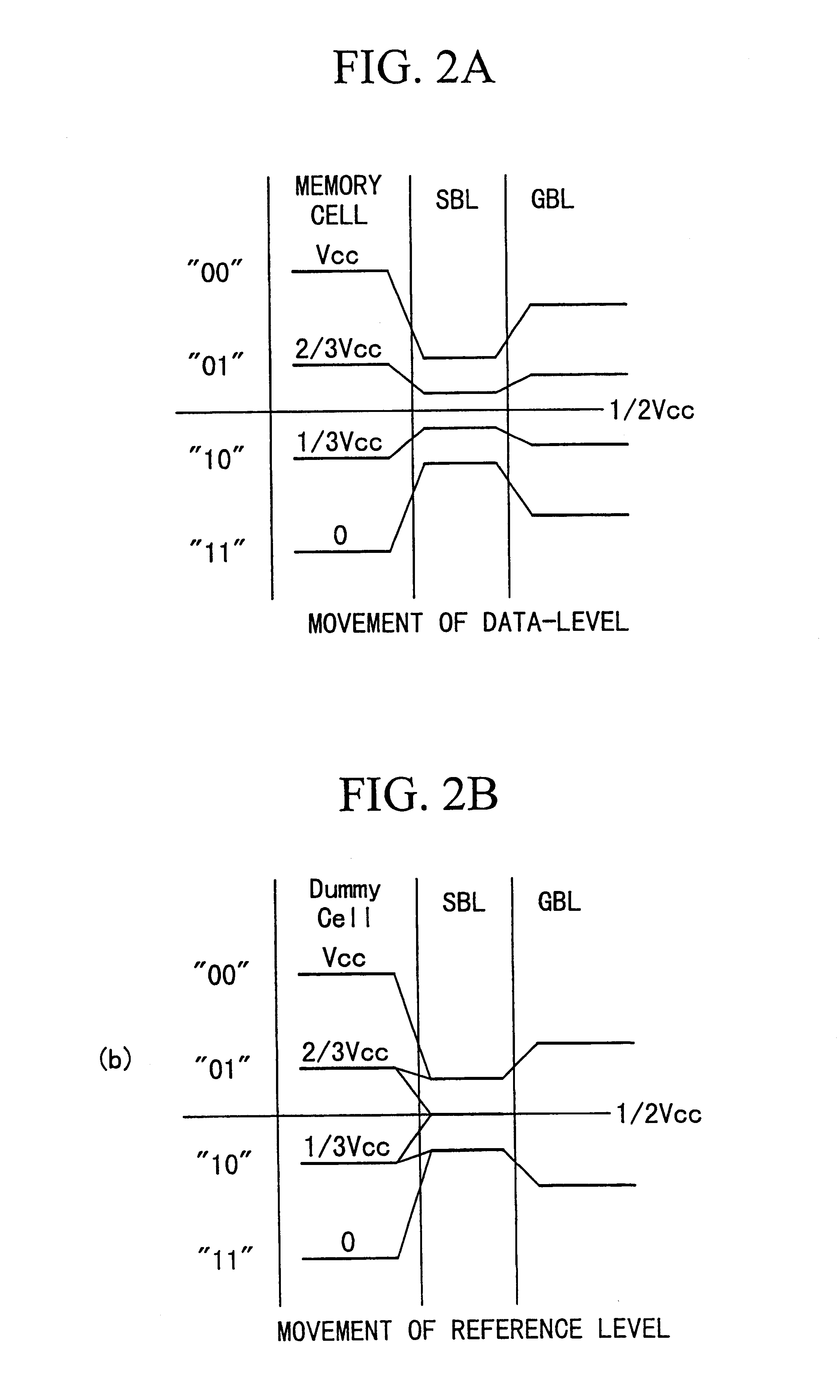
In the DRAM in each of the embodiments of the present invention, the example of a structure wherein a layered bit line structure is used, and it is assumed that one pair of complementary bit lines and 4 pairs of complementary sub-bit lines are treated as a unit. Metal wiring such as aluminum is ...

second embodiment

In the above-described first embodiment, while three stages of sensing are carried out in order to read the multi-level data stored in a memory cell, theoretically, by providing three the MSAs for each of SSAs, reading with a one-stage sensing is possible. However, if this structure is implemented, not only does the printing of the main bit lines become physically problematic, the disposition of the MSAs also becomes troublesome. Thus, it is difficult to say that such a method can be realized. Therefore, in the present embodiment, the three-stage sensing carried out in the first embodiment is reduced to two-stage sensing, and the operation time can be reduced without making the structure excessively complicated.

FIG. 8 is a block diagram showing the structure of the essential elements of the DRAM according to the present embodiment, and structures that are identical to those shown in FIG. 1 (the first embodiment) have identical reference symbols. As shown in the figure, in the presen...

third embodiment

In the above-described second embodiment, sensing is carried out essentially in two stages, but in the present embodiment, by carrying out the sensing in one stage, the operating time can be further reduced. FIG. 13 is a block diagram showing the structure of the essential elements of the DRAM according to the present embodiment, and essential elements of the structure that are the same as those shown in FIG. 8 (the second embodiment) have the same reference symbols. In the present embodiment, twice as many sub-arrays, SSAs, and main bit lines are used as those in the second embodiment, and at the same time, four times as many the MSAs are used as in the second embodiment to carry out access of the memory cells.

Thus, in the present embodiment, for one word line WL, 4 pairs.times.4=16 pairs of sub-bit lines intersect, and 16 memory cells are disposed where they intersect. Similarly, for the dummy word lines DWLT and DWLN, 16 sub-bit lines intersect, and 16 dummy cells are disposed wh...


PUM


Abstract

The present invention provides a multi-value DRAM that does not require additional surface area, has a low cost, and has a good yield. A 4-value memory cell is disposed at the intersection of a word line WL and sub-bit lines BLNx0. A potential corresponding to 11, 10, 01, and 00 is written to the dunmmy cell disposed at the intersection of the sub-bitline connected to the dummy word lines DWLN and DWLT and the SSAs 31 and 32. The SSA30 outputs the data in the memory cell and the reference levels 0x and 1x on the sub-bit lines BLTx0 to the main bit lines GBLN0 and GBLT0. The SSA31 balances the potentials of the dummy cell connected to both dummy word lines and outputs the reference levels 11 and 10 to the main bit line GBLN4. Similarly, the SSA32 balances the potentials of both dummy cells, and outputs the reference levels 01 and 00 to the main bit line GBLT4. The MSA 33 discriminates the upper bit UPBIT and the lower bit LWBIT of the data based on the potentials on the 4 main bit lines.

Description

1. Field of the InventionThe present invention relates to a semiconductor memory device exemplified for example by DRAM (Dynamic Random Access Memory), and in particular to a semiconductor memory device that stores multi-value data having more than two values in a memory cell.2. Description of the Related ArtA 4-value DRAM disclosed in Japanese Unexamined Patent Application, First Publication, No. Hei 9-320280, is a first example of conventional art related to multi-value semiconductor memory devices. FIG. 21 extracts from the structure of the DRAM as a whole one memory cell and a circuit for reading and writing that memory cell, to illustrate the circuit that appears in this publication more schematically. Thus, a summary of the read operation from the memory cell will be described below.Moreover, the memory cell 100 shown in the figure holds a potential depending on the data it stores, and for example, when the electric source potential is VCC, holds 0, (1 / 3) VCC, (2 / 3) VCC, and V...

Claims


Application Information

Patent Timeline
Patent Type & Authority Patents(United States)
IPC IPC(8): G11C11/4091G11C11/409G11C11/56G11C11/401G11C11/407G11C29/04
CPCG11C11/4091G11C11/56G11C11/565G11C7/18G11C16/24
Inventor SUGIBAYASHI, TADAHIKO
Owner NEC ELECTRONICS CORP
Why Eureka
Try Eureka