Multi-value optical transmitter

a multi-value optical transmitter and optical transmission line technology, applied in the field of multi-value optical transmission lines, can solve the problems of increasing the number of mz modulators, increasing the cost of analog electrical parts, and reducing the wavelength dispersion tolerance of optical transmission lines, so as to maximize the average power and maximize the average power. , the effect of stabilizing the dc bias

Active Publication Date: 2011-01-20
MITSUBISHI ELECTRIC CORP
View PDF19 Cites 50 Cited by
  • Summary
  • Abstract
  • Description
  • Claims
  • Application Information

AI Technical Summary

Benefits of technology

[0022]According to the present invention, there is provided a multi-value optical transmitter for converting an input data series which is an input electrical signal into an optical multi-value signal and outputting the optical multi-value signal, including: a first D/A converter for performing D/A conversion on first modulation data set based on the input data series to generate a first multi-value signal; a second D/A converter for performing D/A conversion on second modulation data set based on the input data series to generate a second multi-value signal; a light source; a dual-electrode MZ modulator including: a first phase modulator for modulating light from the light source based on the first multi-value signal; and a second phase modulator for modulating the light from the light source based on the s

Problems solved by technology

When a symbol rate of symbols transmitted to an optical transmission line is increased without changing a modulation method, there is a problem in that wavelength dispersion tolerance of the optical transmission line reduces because an allowable residual dispersion amount is inversely proportional to the square of the symbol rate.
It is necessary to execute electrical signal processing at high speed, and hence there is a problem in that the cost of an analog electrica

Method used


Image

  • Multi-value optical transmitter
  • Multi-value optical transmitter
  • Multi-value optical transmitter

Examples


embodiment 1

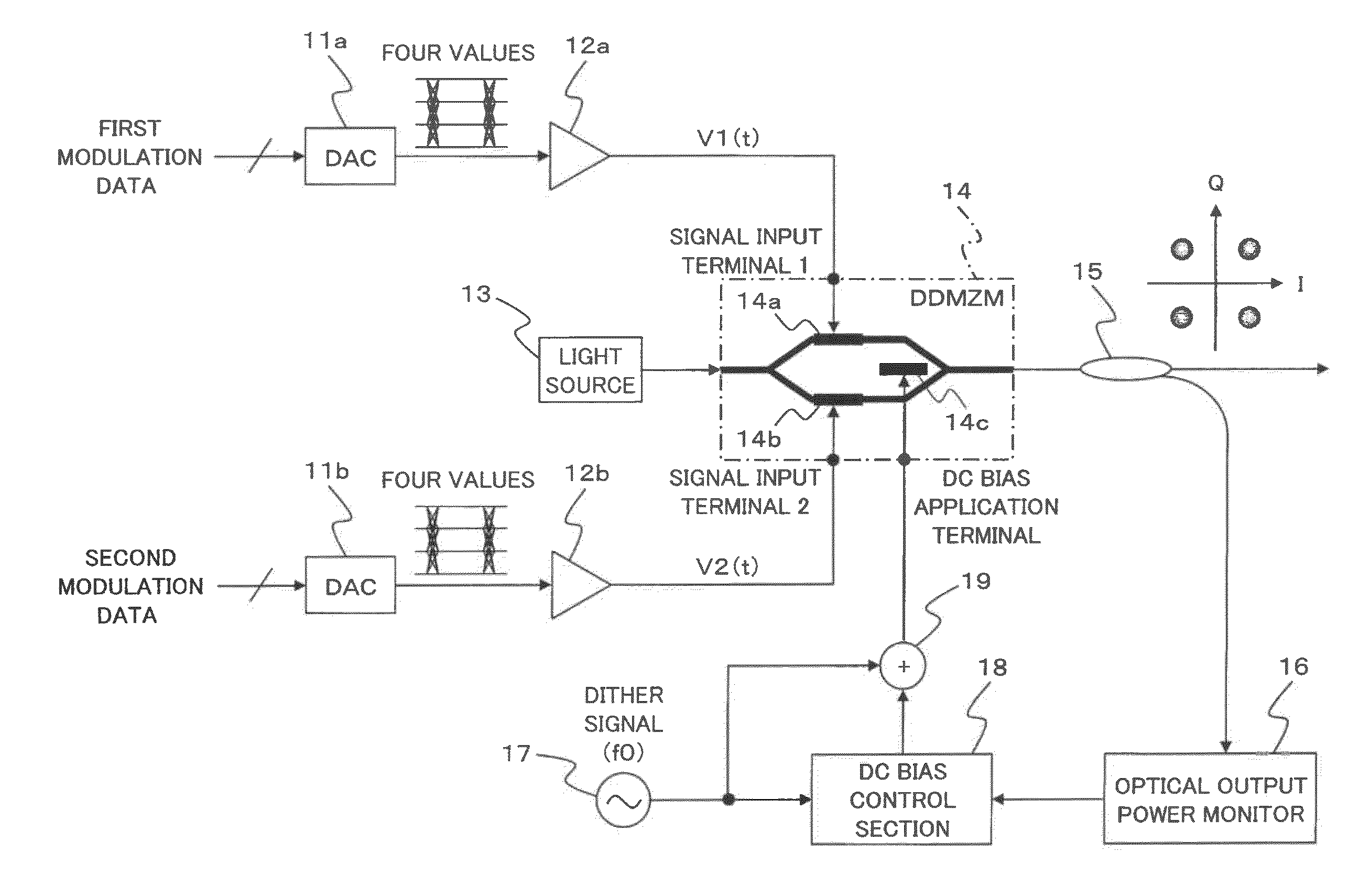
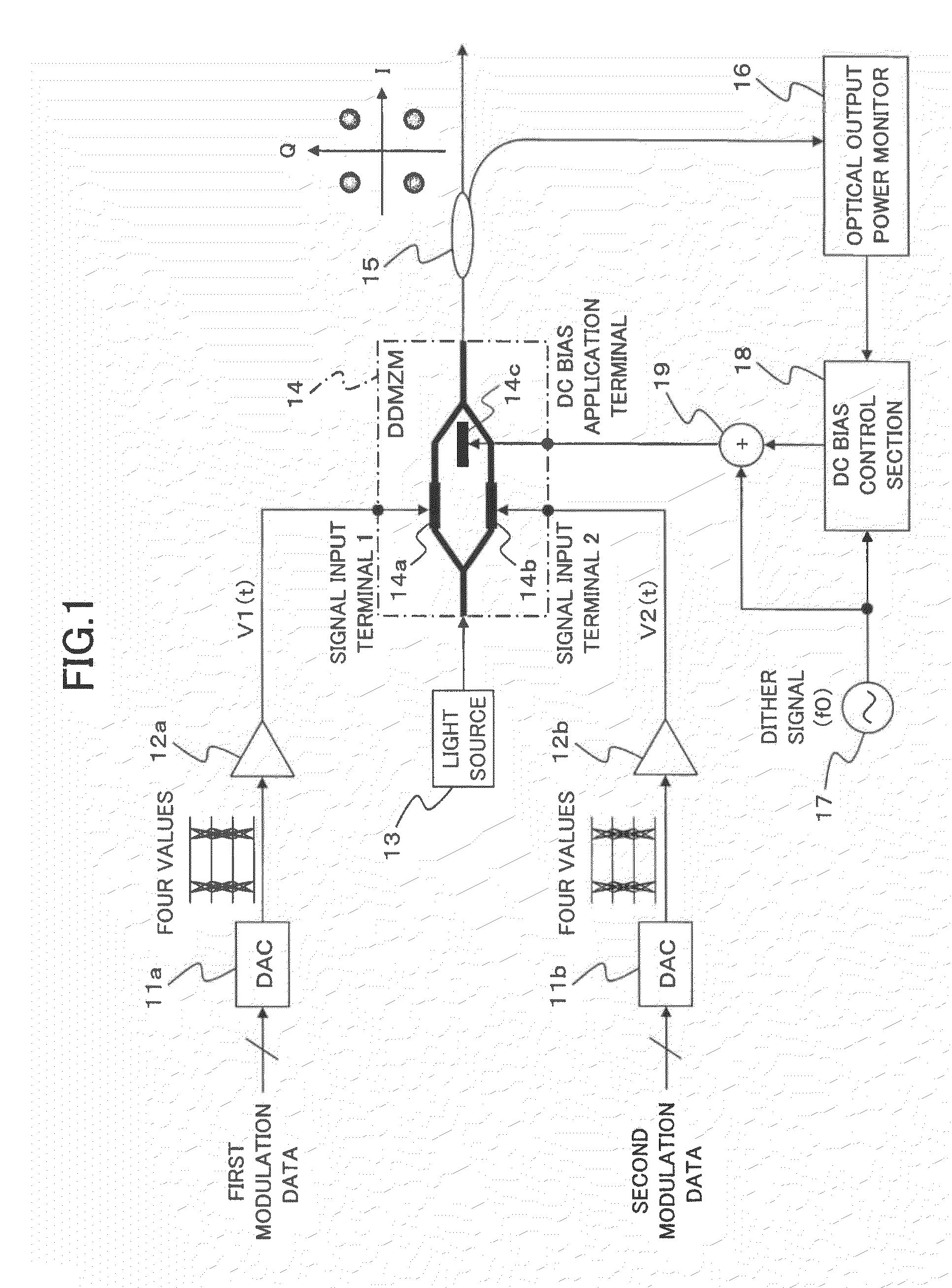
[0034]FIG. 1 is a block structural diagram illustrating a multi-value optical transmitter according to Embodiment 1 of the present invention.

[0035]In FIG. 1, the multi-value optical transmitter includes two D / A converters (first and second D / A converters) 11a and 11b, two electrical amplifiers 12a and 12b, a light source 13, a dual-electrode MZ modulator (DDMZM) 14, an optical tap coupler 15, an optical output power monitor (power monitor means) 16, an oscillator 17, a DC bias control section 18, and an adder 19.

[0036]The dual-electrode MZ modulator 14 includes two phase modulators (first and second phase modulators) 14a and 14b and an electrode 14c for bias. A first signal input terminal, a second signal input terminal, and a DC bias application terminal are provided in the dual-electrode MZ modulator 14 and connected to the phase modulator 14a, the phase modulator 14b, and the electrode 14c, respectively. The oscillator 17, the DC bias control section 18, and the adder 19 serve as...


PUM


Abstract

Provided is a multi-value optical transmitter in which a DC bias may be controlled to be stabilized so as to obtain stable optical transmission signal quality in multi-value modulation using a dual-electrode MZ modulator. The multi-value optical transmitter includes: D/A converters for performing D/A conversion on first and second modulation data which are set based on an input data series, so as to generate a first and a second multi-value signal, respectively; a dual-electrode MZ modulator including phase modulators for modulating light from a light source based on the first multi-value signal and the second multi-value signal, so as to combine optical signals from the phase modulators to output the optical multi-value signal; an optical output power monitor for detecting average power of the optical multi-value signal; and a DC bias control unit for controlling a DC bias for the dual-electrode MZ modulator, so as to maximize the average power.

Description

BACKGROUND OF THE INVENTION[0001]1. Field of the Invention[0002]The present invention relates to a multi-value optical transmitter for converting an electrical signal into an optical signal and transmitting the optical signal.[0003]2. Description of the Related Art[0004]In order to realize a large capacity of a wavelength division multiplex (WDM) optical communication system, it is useful to increase a transmission rate per wavelength. When a symbol rate of symbols transmitted to an optical transmission line is increased without changing a modulation method, there is a problem in that wavelength dispersion tolerance of the optical transmission line reduces because an allowable residual dispersion amount is inversely proportional to the square of the symbol rate. It is necessary to execute electrical signal processing at high speed, and hence there is a problem in that the cost of an analog electrical part increases.[0005]Therefore, in recent years, researches for improving signal mu...

Claims


Application Information

Patent Timeline
IPC IPC(8): H04B17/00G02F1/03H04B10/07H04B10/293H04B10/516H04B10/556H04B10/564H04B10/572H04B10/61
CPCG02F1/0123H04B10/564H04B10/50575G02F1/2255
Inventor SUGIHARA, TAKASHIKAMETANI, SOICHIROMIZUOCHI, TAKASHI
Owner MITSUBISHI ELECTRIC CORP
Why Eureka
Try Eureka