Semiconductor device and fabrication method of the same

a technology of semiconductors and semiconductors, applied in the direction of semiconductor devices, electrical equipment, transistors, etc., can solve the problems of difficult enlarging size, high breakdown voltage cannot be achieved, and high cost of gan substrates, and achieve low on-state resistance and high breakdown capability.

Inactive Publication Date: 2006-10-05
SUMITOMO ELECTRIC DEVICE INNOVATIONS
View PDF13 Cites 24 Cited by
  • Summary
  • Abstract
  • Description
  • Claims
  • Application Information

AI Technical Summary

Benefits of technology

[0008] The present invention has been made in view of the above circumstances, and has an object to provide a semiconductor device having a high breakdown capability and a low on-state resistance.

Problems solved by technology

However, the first prior art has a problem such that the SiC channel layer realizes a mobility of only tens of cmV / s and the resultant on-state resistance. is as low as tens of mΩ / cm2.
The second prior art has a problem such that high breakdown voltage cannot be achieved-because the drain electrode is connected to the drain layer.
However, the GaN substrate is very expensive and has a difficulty in enlarging the size.
For a substrate that does not have lattice match with the GaN layer, GaN cannot be grown to form a thick film, and high breakdown cannot be achieved.

Method used


Image

  • Semiconductor device and fabrication method of the same
  • Semiconductor device and fabrication method of the same
  • Semiconductor device and fabrication method of the same

Examples


first embodiment

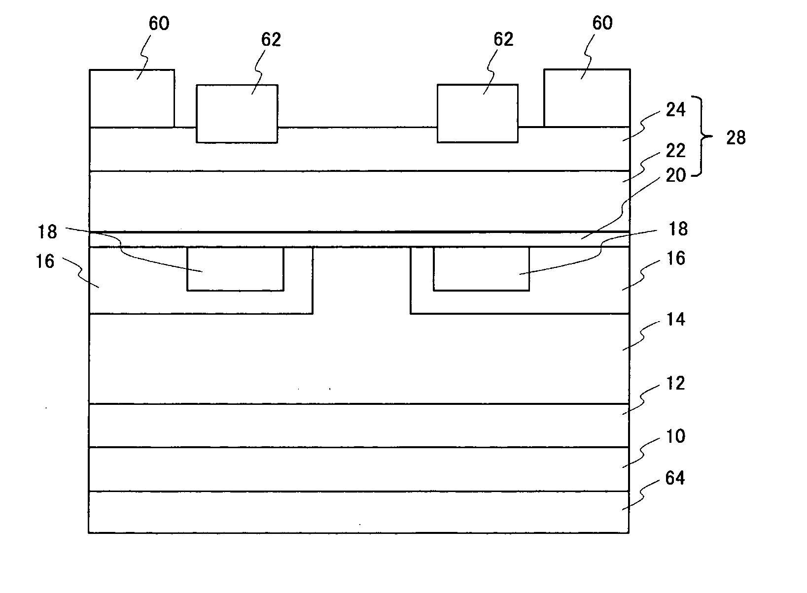
[0036]FIG. 2 is a cross-sectional view of a transistor in accordance with a first embodiment of the present invention. This transistor is a vertical type FET (HEMT: High Electron Mobility Transistor). The aforementioned n-type SiC buffer layer 12 and the n-type SiC drift layer 14 are formed on a (0001) plane of the n-type SiC substrate 10 in this order. Further, an n-type AlGaN layer 20, a GaN channel layer 22 and an AlGaN cap layer 24 are grown as a GaN-based semiconductor layer 28. The source electrodes 60 are formed on the cap layer 24, and gate electrodes 62 are partially buried in the cap layer 24. P-type SiC regions 16 are provided in the drift layer 14 below the gate electrodes 62, and highly doped p-type SiC regions 18 are provided in the drift layer 14. A drain electrode 64 is provided on the backside of the SiC substrate 10. That is, the drain electrode 64 is formed on a surface that opposes the GaN-based semiconductor layer across the SiC layer. The transistor of the firs...

second embodiment

[0048]FIG. 8 is a cross-sectional view of a transistor in accordance with a second embodiment of the present invention. This transistor is a vertical type FET (HEMT). The n-type SiC buffer layer 12 and then-type SiC drift layer 14 are formed on the (0001) plane of the n-type SiC substrate 10 in this order. As the GaN-based semiconductor layer 38, an n-type AlGaN drain layer 30, a p-type GaN channel layer (p-type GaN-based semiconductor layer) 32, and an AlGaN source layer 34. An opening region 37 is formed so as to reach the AlGaN drain layer 30 from the device surface. The opening region 37 is essentially deeper than the p-type channel layer 32.

[0049] An AlN cap layer 36 is formed so as to cover the opening region 37. Gate electrodes 60 are formed on the cap layer 36, and the source electrodes 60 are on the cap layer 36, namely, the GaN-based semiconductor layer 38. The cap layer 36 having a wider band gap than that of the channel layer 32 is arranged on the side surface of the ch...

third embodiment

[0056]FIG. 13 is a cross-sectional view of a transistor in accordance with a third embodiment of the present invention. This transistor is a vertical FET (HEMT). The n-type SiC buffer layer 12, the n-type SiC drift layer 14 and the p-type SiC layer 15 are formed on the (0001) plane of the n-type SiC substrate 10 in this order. An opening region 47 is formed so as to be at least deeper than the p-type SiC layer 15. As a GaN-based semiconductor layer 48, an n-type AlGaN drain layer 40, a p-type GaN channel layer 42 and an AlGaN source layer 44 are formed in this order. The GaN-based semiconductor layer 48 has a resultant opening region.

[0057] The source electrodes 60 are formed on the source layer 44, and the gate electrodes 62 are partially buried in the source layer 44. The drain electrode 64 is formed on the backside of the SiC substrate 10. That is, the drain electrode 64 is connected to the surface of the drift layer 14 that opposes the GaN-based semiconductor layer 48 across th...


PUM


Abstract

A semiconductor device includes a substrate, a SiC drift layer formed above the substrate, a GaN-based semiconductor layer that is formed on the SiC drift layer and includes a channel layer, a source electrode and a gate electrode formed on the GaN-based semiconductor layer, current blocking regions formed in portions of the SiC drift layer and located below the source and gate electrodes, and a drain electrode formed on a surface that opposes the GaN-based semiconductor layer across the SiC layer.

Description

BACKGROUND OF THE INVENTION [0001] 1. Field of the Invention [0002] The present invention generally relates to semiconductor devices and fabrication methods of the same, and more particularly, to a power control transistor having a vertical structure and a method of fabricating the same. [0003] 2. Description of the Related Art [0004] The power control transistors are widely used in various fields such as home electric appliances, electric railways, electric automobiles and electric power. The power control transistors are required to have high breakdown capability such that dielectric breakdown does not take place even if high power is applied. The power control transistors are also required to have a small on-state resistance in order to realize low insertion loss. Recently, transistors having a vertical structure have had a great deal of attention as power control transistors. [0005]FIG. 1 is a cross-sectional view of a Si-based vertical type MOSFET (hereinafter referred to as fi...

Claims


Application Information

Patent Timeline
Patent Type & Authority Applications(United States)
IPC IPC(8): H01L31/00H01L29/06H01L21/337H01L21/338H01L29/12H01L29/739H01L29/778H01L29/78H01L29/808H01L29/812
CPCH01L29/7789H01L29/802H01L29/1029H01L29/1608H01L29/7788H01L29/267H01L29/66462H01L29/7395H01L29/7783H01L29/2003H01L29/0646H01L29/7397
Inventor KAWASAKI, TAKESHINAKATA, KENYAEGASHI, SEIJI
Owner SUMITOMO ELECTRIC DEVICE INNOVATIONS
Why Eureka
Try Eureka