Split gate structure, power mos device, and manufacturing method

a technology of split gate and power mos, which is applied in the field of split gate structure and power mos device, can solve the problems of split gate power mos igss performance and power consumption of electric devices, and achieve the effect of improving breakdown performance and igss performance of split gate power mos

Active Publication Date: 2021-09-23
HEJIAN TECH SUZHOU
View PDF0 Cites 2 Cited by
  • Summary
  • Abstract
  • Description
  • Claims
  • Application Information

AI Technical Summary

Benefits of technology

[0004]In order to solve the existing technical problem, a split gate structure which can effectively improve the breakdown performance and the IGSS performance, a power MOS device having the same, and a manufacturing method of the same are provided in the present invention.
[0018]Since the technical solutions as described above are adopted, the present invention has the following advantages over the existing technology. Compared to a conventional split gate structure, in the new split gate structure fabricated by the manufacturing method of a split gate structure according to the present invention, the flatness of the contact surface between the characteristic oxide and the polysilicon is improved, and thereby the effective distance between the first polysilicon and the second polysilicon is increased. As such, the breakdown performance and the IGSS performance of the split gate power MOS are effectively improved.

Problems solved by technology

When the device is turned off, it is preferable to have a small leakage, otherwise, the electric device will be power consuming.
Therefore, the improvement of the breakdown performance and the IGSS performance of a split gate power MOS becomes a problem to be solved in the technical field of semiconductor.

Method used


Image

  • Split gate structure, power mos device, and manufacturing method
  • Split gate structure, power mos device, and manufacturing method
  • Split gate structure, power mos device, and manufacturing method

Examples


Embodiment Construction

[0025]The present invention will be described in detail through the following embodiments with appending drawings such that the objectives, technical solutions, and advantages of the present invention will be more clear. It should be understood that the specific embodiments are provided for an illustrative purpose only, and should not be interpreted in a limiting manner.

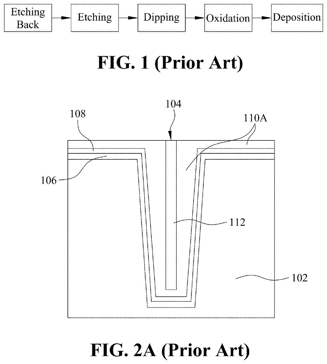
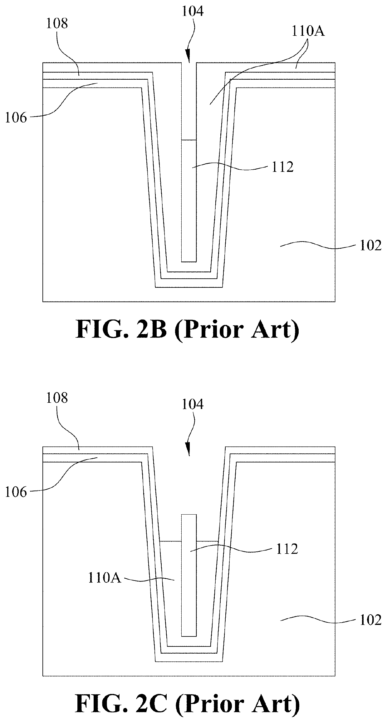
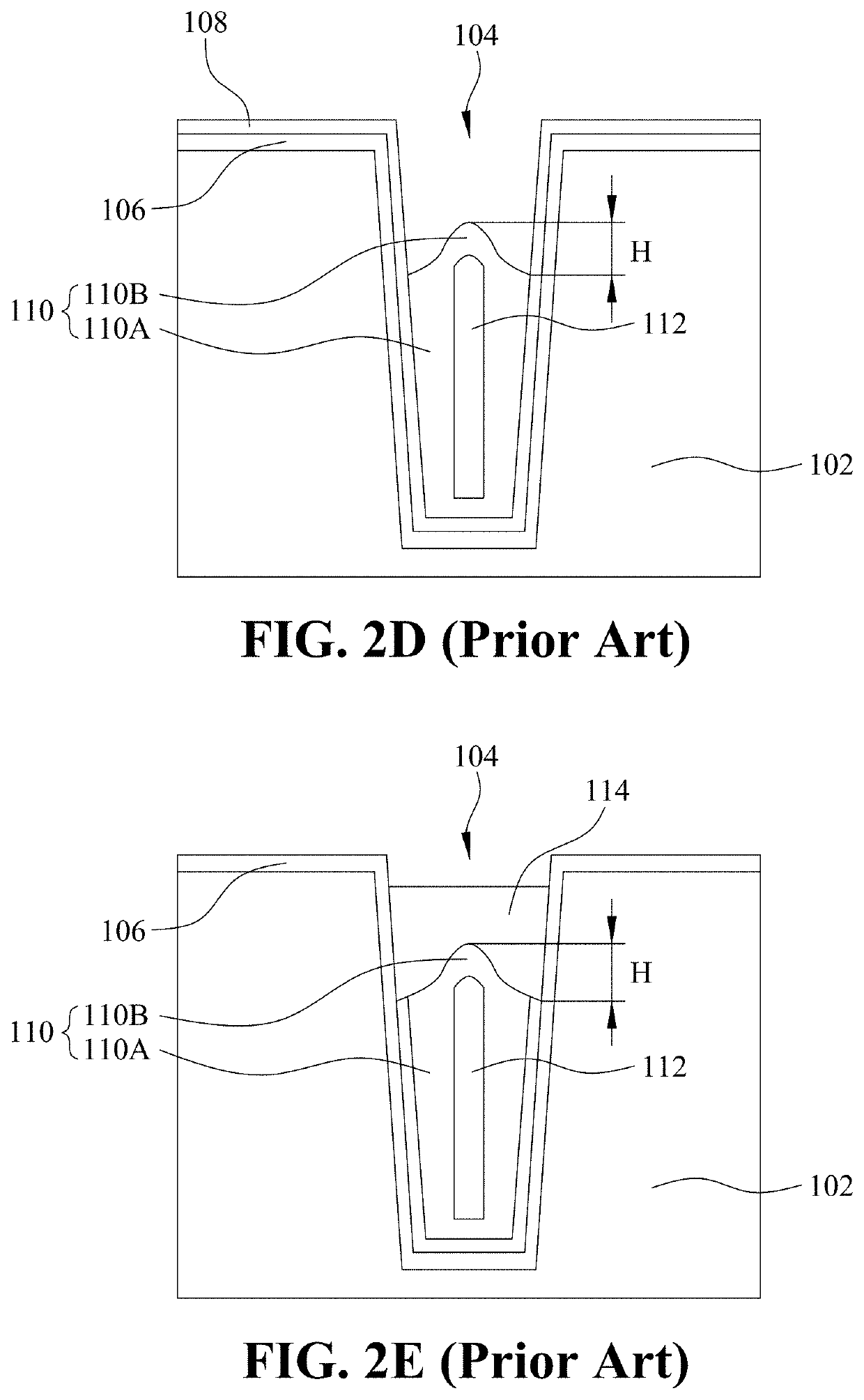
[0026]As illustrated in FIG. 1 and FIGS. 2A-2E, a conventional manufacturing method typically comprises the processes of etching back-etching-dipping-oxidation-deposition. Specifically, an etching back process is firstly performed on a first polysilicon 112 in a trench 104 with a characteristic oxide 110A on a wall thereof such that the first polysilicon 112 has a height higher than a depth of the trench 104 (FIG. 2A). Then, a first etching process is performed on the first polysilicon 112 such that the first polysilicon 112 has a height lower than the depth of the trench 104 (FIG. 2B). A dipping step is performed, i...


PUM

PropertyMeasurementUnit
heightaaaaaaaaaa
distanceaaaaaaaaaa
heightaaaaaaaaaa

Abstract

A split gate structure is disclosed. The split gate structure includes a first polysilicon, a characteristic oxide, and a second polysilicon sequentially disposed in a trench in a vertical direction upward from a bottom of the trench. An upper surface of the characteristic oxide has a height difference less than 1500 Å between a higher center portion and a lower periphery portion. The split gate structure effectively improves the breakdown performance and the IGSS performance. A power MOS device having the split gate structure and a manufacturing method of the split gate structure are also provided.

Description

CROSS-REFERENCE TO RELATED APPLICATION[0001]This application claims the priority of CN patent application No. 202010193258.3, filed on Mar. 18, 2020, which is incorporated herewith by reference.BACKGROUND OF THE INVENTION1. Field of the Invention[0002]The present invention relates to the technical field of semiconductor, particularly to a split gate structure which can effectively improve the breakdown performance and the IGSS performance, a power MOS device, and a manufacturing method.2. The Prior Arts[0003]Generally, a split gate power MOS (split gate power FET) is used as a switching device in an integrated circuit. When the device is turned off, it is preferable to have a small leakage, otherwise, the electric device will be power consuming. As such, the IGSS performance and the breakdown performance are important parameters for evaluating the performance of a split gate power MOS. Therefore, the improvement of the breakdown performance and the IGSS performance of a split gate p...

Claims


Application Information

Patent Timeline
Patent Type & Authority Applications(United States)
IPC IPC(8): H01L29/40H01L29/423H01L21/28H01L21/765H01L21/3213H01L21/02
CPCH01L29/407H01L29/4236H01L29/42376H01L21/02255H01L21/765H01L21/32133H01L21/28114H01L29/42368H01L21/28008H01L29/7827H01L21/28035H01L21/28247H01L29/66734
Inventor ZHENG, YUAN CHENGSHI, XIN HUAN
Owner HEJIAN TECH SUZHOU
Why Eureka
Try Eureka