LED package using Si substrate and fabricating method thereof

a technology of led packaging and substrate, which is applied in the direction of electrical equipment, semiconductor devices, control devices, etc., can solve the problems of large amount of heat generated by led, degraded led characteristics, and increased consumption of power, and achieve the effect of dissipating heat generated

Inactive Publication Date: 2006-10-05
SAMSUNG ELECTRONICS CO LTD
View PDF5 Cites 80 Cited by
  • Summary
  • Abstract
  • Description
  • Claims
  • Application Information

AI Technical Summary

Benefits of technology

[0011] An object of the present invention is to provide an LED package using a Si substrate that is constructed to effectively dissipate heat generated from a high-brightness,. high-power LED by forming a heat dissipating unit on one side of the Si substrate opposite to the other side on which the LED is mounted.

Problems solved by technology

Meanwhile, for applications (e.g., lighting devices) requiring high brightness, the LED consumes more power and thus a large amount of heat is generated from the LED.
If the generated heat is not effectively dissipated, characteristics of the LED may be degraded or lifespan of the LED may be reduced.
However, this method has a limitation in improving the heat dissipating efficiency.
Therefore, even the use of Si substrates with good heat conductivity cannot solve the thermal degradation of the LED characteristics and the reduction in the lifespan of the LED.

Method used


Image

  • LED package using Si substrate and fabricating method thereof
  • LED package using Si substrate and fabricating method thereof
  • LED package using Si substrate and fabricating method thereof

Examples


Embodiment Construction

[0030] Reference will now be made in detail to the preferred embodiments of the present invention, examples of which are illustrated in the accompanying drawings. The invention may, however, be embodied in many different forms and should not be construed as being limited to the embodiments set forth herein; rather, these embodiments are provided so that this disclosure will be thorough and complete, and will fully convey the concept of the invention to those skilled in the art. In the drawings, the thicknesses of layers and regions are exaggerated for clarity, and like reference numerals denote like elements.

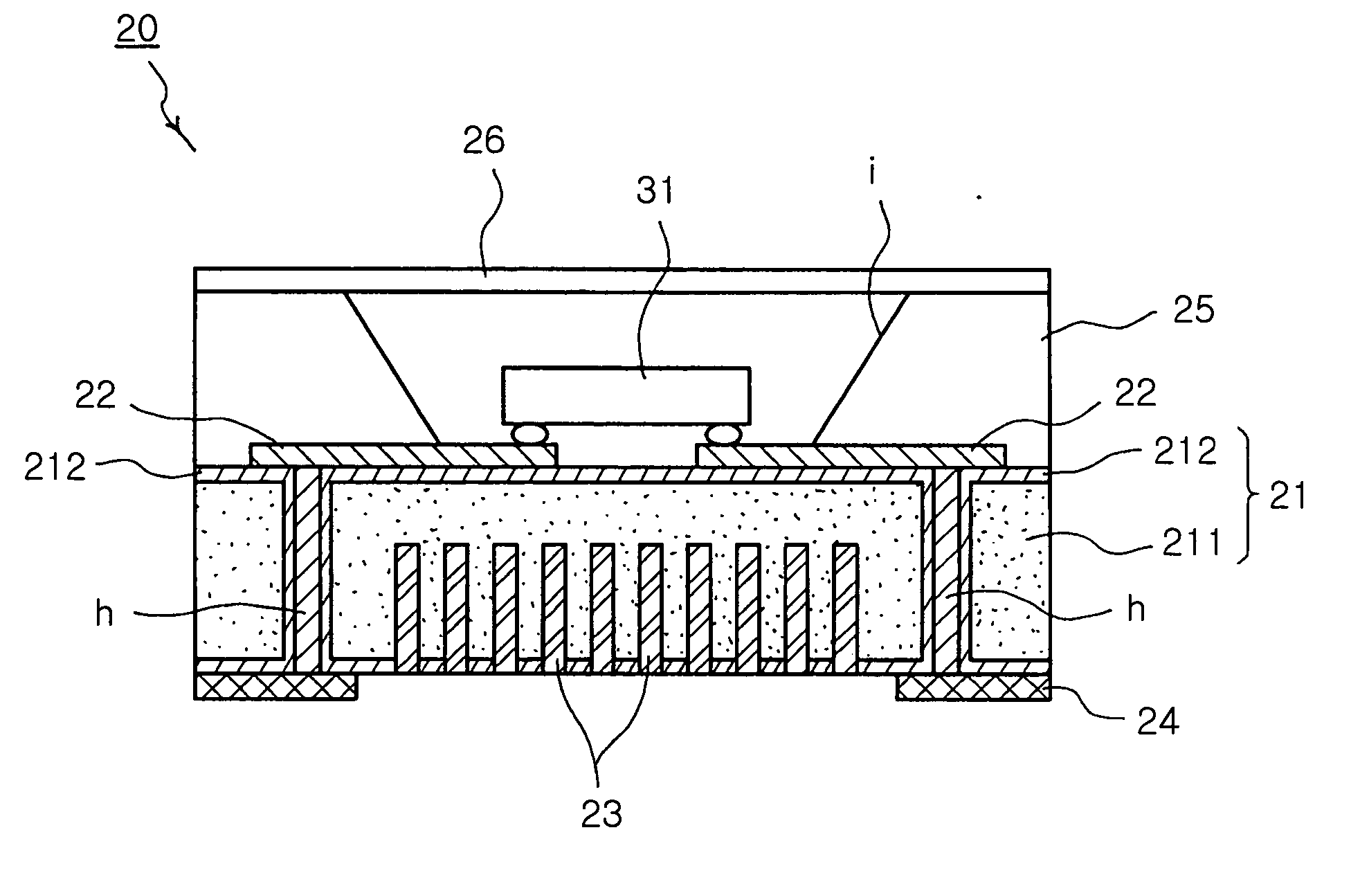
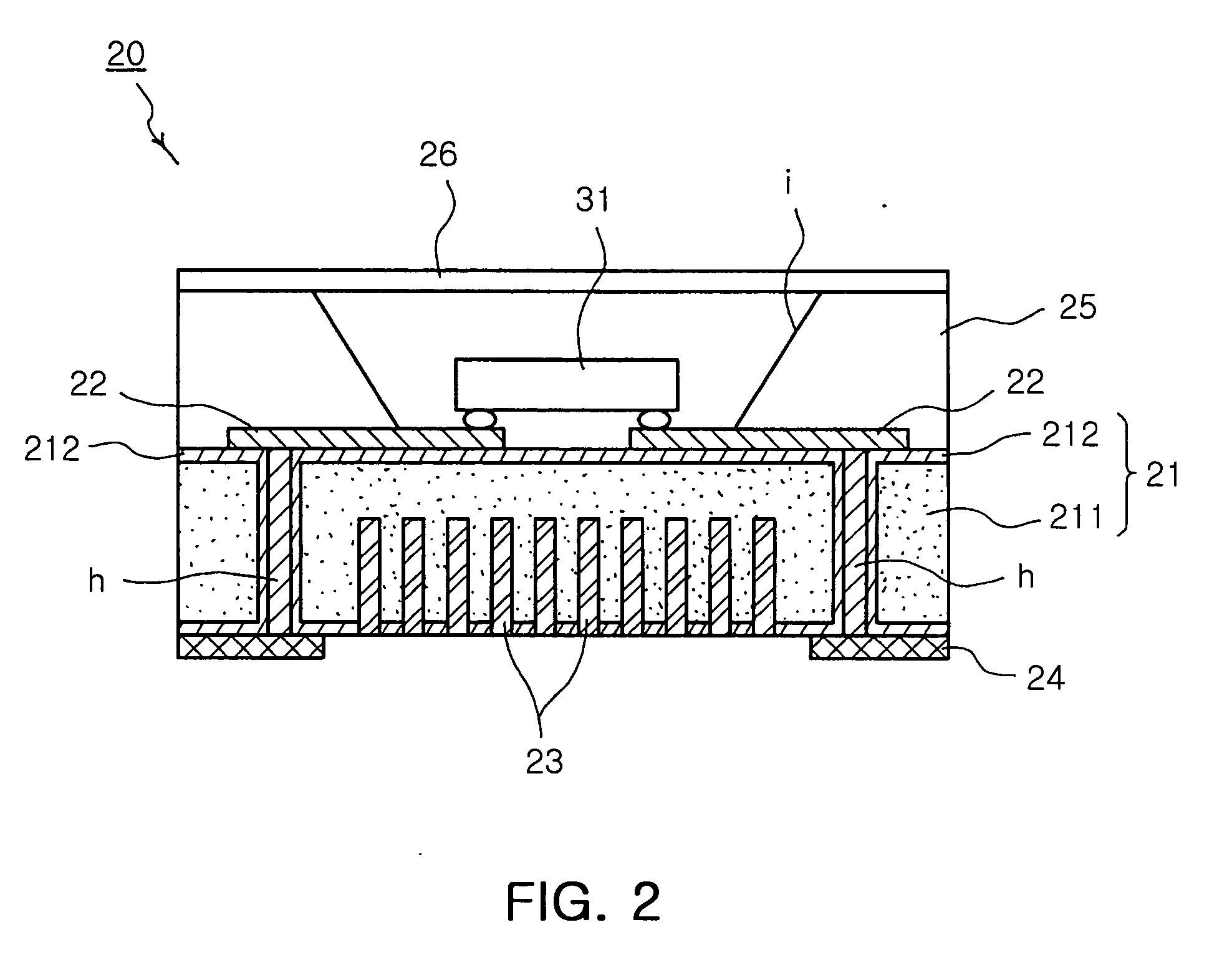
[0031]FIG. 2 is a sectional view of an LED package according to an embodiment of the present invention. Referring to FIG. 2, an LED package 20 using a Si substrate according to an embodiment of the present invention includes a Si substrate 211, insulating layers 212 formed on top and bottom surfaces of the Si substrate 211, a supporting structure 21 having at least one groove f...


PUM


Abstract

There are provided an LED package using a Si substrate and a fabricating method of the LED package. In the LED package, a supporting structure includes a Si substrate and an insulating layer formed on top and bottom surfaces of the Si substrate, and the supporting structure defines at least one groove in a bottom surface by partially removing the Si substrate and the insulating layer. A plurality of upper electrodes is formed on a top surface of the supporting structure. At least one LED is mounted on the top surface of the supporting structure, and the LED includes both terminals electrically connected to the upper electrodes. A metal filler is filled in the groove defined in the bottom surface of the supporting structure.

Description

RELATED APPLICATION [0001] The present application is based on, and claims priority from, Korean Application Number 2005-26515, filed Mar. 30, 2005, the disclosure of which is hereby incorporated by reference herein in its entirety. BACKGROUND OF THE INVENTION [0002] 1. Field of the Invention [0003] The present invention relates to an LED package using a Si substrate and a fabricating method of the LED package, and more particularly, to an LED package using a Si substrate in which a metallic heat dissipating unit is provided in a side opposite to a side on which an LED is mounted to effectively dissipate heat generated from the LED to the outside for preventing degradation of the LED and increasing the lifespan of the LED, and a fabricating method of the LED package. [0004] 2. Description of the Related Art [0005] Light emitting diode (LED) is a diode that emits light using energy generated when injected electrons and holes are recombined. Examples of the LED are red LEDs using GaAs...

Claims


Application Information

Patent Timeline
Patent Type & Authority Applications(United States)
IPC IPC(8): H01L33/00H01L33/44H01L33/58H01L33/60H01L33/62H01L33/64
CPCH01L33/486H01L33/642H01L2224/48091H01L2224/16225H01L2224/48227H01L2924/00014H01L2924/00011H01L2224/0401B60W40/09B60W50/14B60W2050/143B60W2050/146
Inventor LEE, SUNG JUNHWANG, WOONG LINCHOI, SANG HYUNLIM, CHANG HYUNPARK, HO JOONCHOI, SEOG MOON
Owner SAMSUNG ELECTRONICS CO LTD
Why Eureka
Try Eureka