Semiconductor device having GaN-based semiconductor layer

a semiconductor layer and semiconductor technology, applied in the field of semiconductor devices, can solve the problems of reducing drain current (collapse phenomenon) and difficult high-output operations, and achieve the effect of inhibiting the collapse phenomenon, high-output operations, and high-output operations

Active Publication Date: 2006-10-05
EUDYNA DEVICES INC
View PDF4 Cites 80 Cited by
  • Summary
  • Abstract
  • Description
  • Claims
  • Application Information

AI Technical Summary

Benefits of technology

[0016] According to a still further aspect of the present invention, there is provided a substrate used to fabricate a semiconductor device including a GaN-based semiconductor layer formed on a base substrate, and an insulating film, composed of any one of silicon nitride in which the composition ratio of silicon to nitrogen is 0.85 to 3.0, silicon oxide in which the composition ratio of silicon to oxygen is 0.6 to 3.0, or silicon oxide nitride in which the composition ratio of silicon to nitrogen and oxygen is 0.6 to 3.0, formed on a surface of the GaN-based semiconductor layer. It is thus possible to reduce an oxide of a Group III element that is formed within the semiconductor layer between the gate electrode and the drain electrode and causes the collapse phenomenon, and to inhibit the collapse phenomenon. Thus, a substrate used to fabricate a semiconductor device that is used to fabricate a semiconductor device capable of high output operations can be provided. Furthermore, a substrate used to fabricate a semiconductor device that is suitable for storage can be provided.
[0017] According to another aspect of the present invention, there is provided a substrate used to fabricate a semiconductor device including a GaN-based semiconductor layer formed on a base substrate, and an insulating film, composed of either aluminum nitride in which the composition ratio of aluminum to nitrogen is 1.2 to 2.0 or aluminum oxide in which the composition ratio of aluminum to oxygen is 0.7 to 2.0, formed on the surface of the GaN-based semiconductor layer. In accordance with the present invention, an oxide of a Group III element that is formed within the semiconductor surface layer between the gate electrode and the drain electrode and causes the collapse phenomenon can be reduced, thereby inhibiting the collapse phenomenon. Thus, a substrate used to fabricate a semiconductor device that is used to fabricate of a semiconductor device capable of high output operations can be provided. Furthermore, a substrate used to fabricate a semiconductor device that is suitable for storage can be provided.
[0018] According to another aspect of the present invention, there is provided a method of fabricating a substrate used to fabricate a semiconductor device including a step of forming a GaN-based semiconductor layer on a substrate, and a step of forming an insulating film, composed of any one of silicon nitride in which the composition ratio of silicon to nitrogen is 0.85 to 3.0, silicon oxide in which the composition ratio o

Problems solved by technology

However, in a conventional nitride semiconductor HEMT, a phenomena where drain current decreases (collapse phenomenon) becomes a problem when high drain voltage is applied.
Further, when a drain voltage of 50 V is applied

Method used


Image

  • Semiconductor device having GaN-based semiconductor layer
  • Semiconductor device having GaN-based semiconductor layer
  • Semiconductor device having GaN-based semiconductor layer

Examples


first embodiment

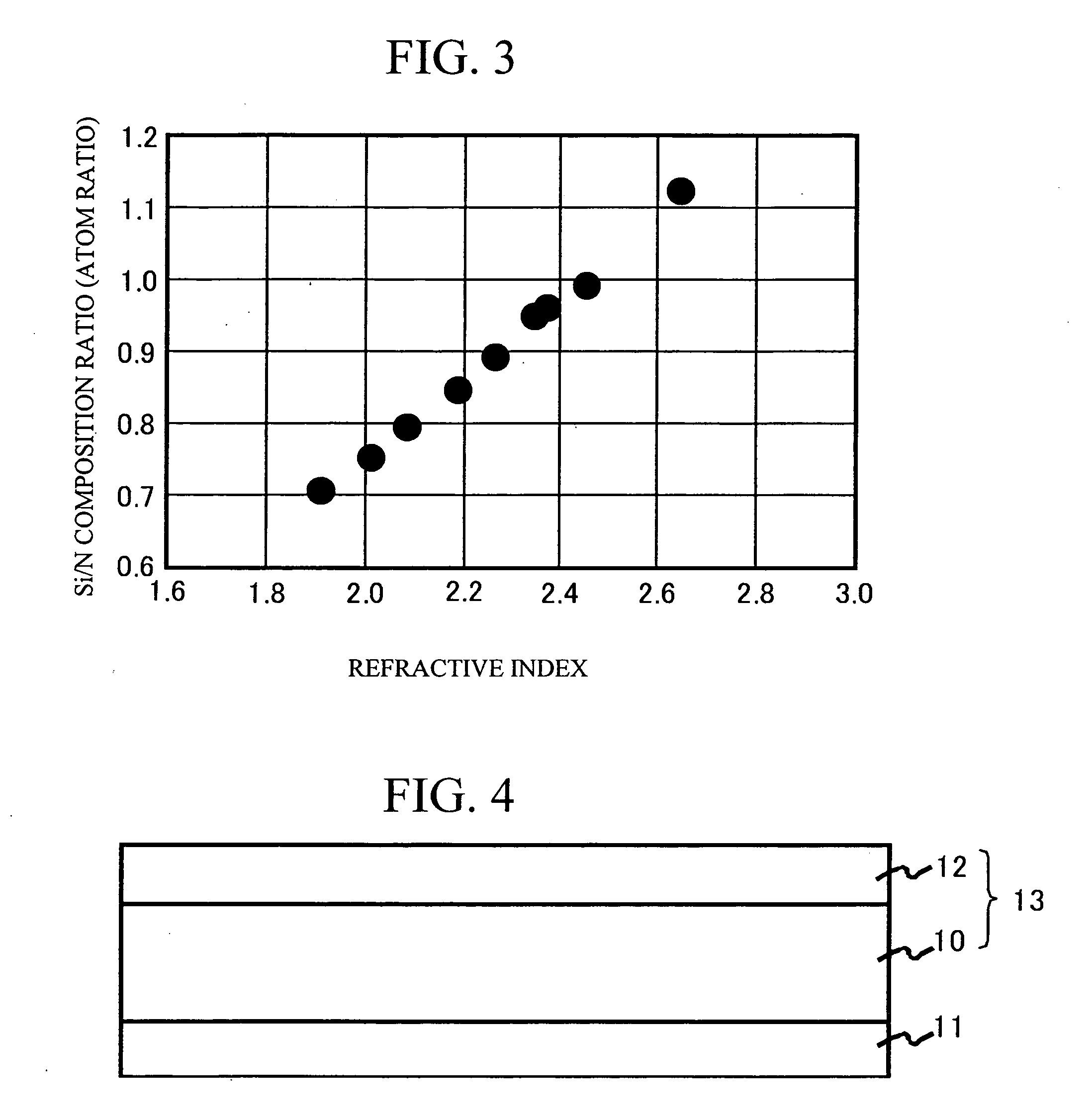
[0037] A first embodiment is an example of the nitride semiconductor HEMT in which a silicon nitride film layer with a refractive index of 2.2 to 2.3, or in other words, with a silicon / nitrogen composition ratio of 1.85 to 1.9, is formed on the semiconductor surface 12 as the insulating film layer 25.

[0038] Hereafter, a fabricating method of the nitride semiconductor HEMT is explained. In FIG. 4, an impurity-free GaN electron transit layer serving as the GaN-based semiconductor layer 13, the semiconductor layer 10 including an Si-added, N-type AlGaN electron supply layer, and a GaN cap layer serving as the semiconductor surface layer 12 are formed on, for example, the SiC substrate 11 using the MOCVD method. Thus, an epitaxial substrate is completed. The silicon nitride film layer with the refractive index of 2.2 to 2.3 is formed on the surface of the semiconductor surface layer 12 as an insulating film layer 25. This silicon nitride film has a silicon / nitride composition ratio of ...


PUM


Abstract

A semiconductor device includes a GaN-based semiconductor layer formed on a substrate, and an insulating film composed of any one of silicon nitride in which the composition ratio of silicon to nitrogen is 0.85 to 3.0, silicon oxide in which the composition ratio of silicon to oxygen is 0.6 to 3.0, or silicon oxide nitride in which the composition ratio of silicon to nitrogen and oxygen is 0.6 to 3.0 that is formed on a surface of the GaN-based semiconductor layer, a gate electrode formed on the GaN-based semiconductor layer, and a source electrode and a drain electrode formed with the gate electrode therebetween.

Description

BACKGROUND OF THE INVENTION [0001] 1. Field of the Invention [0002] The present invention relates to a semiconductor device, a fabricating method thereof, a substrate used to fabricate the semiconductor device, and a fabricating method thereof. More particularly, the present invention relates to a nitride semiconductor device, a fabricating method thereof, a substrate used to fabricate the semiconductor device, and a fabricating method thereof. [0003] 2. Description of the Related Art [0004] A nitride semiconductor, particularly a semiconductor device using gallium nitride (GaN), is used as a power device operating at a high frequency and high output. In particular, a high electron mobility transistor (HEMT) is known as a semiconductor device suitable for performing amplification of high-frequency bandwidths in microwaves, quasi-millimeter waves, millimeter waves, etc. Technology enabling the HEMT to operate under high drain voltage is being developed to allow operation of the HEMT ...

Claims


Application Information

Patent Timeline
IPC IPC(8): H01L29/739
CPCH01L29/812H01L29/2003H01L29/7787
Inventor KURACHI, SHUNSUKEKOMATANI, TSUTOMU
Owner EUDYNA DEVICES INC
Why Eureka
Try Eureka