Fin-type channel transistor and method of manufacturing the same

a transistor and channel technology, applied in transistors, semiconductor devices, electrical equipment, etc., can solve the problems of introducing impurities under, limiting this method, and reducing the effect of parasitic resistance,

Inactive Publication Date: 2006-10-05
KK TOSHIBA
View PDF3 Cites 82 Cited by
  • Summary
  • Abstract
  • Description
  • Claims
  • Application Information

AI Technical Summary

Benefits of technology

[0014] The present invention is proposed in consideration of the aforementioned circumstances, and it is an object of the present invention to provide a Fin-type channel tran...

Problems solved by technology

However, some point out the limitations of this method.
Countermeasures to short channel effect and a decrease in parasitic resistance are considered to be serious problems.
However, because of the structural complication, there are the following three problems arising in the process of manufacturing a Fin-type channel transistor.
First, when an extension layer, a halo layer, and a deep region are formed by ion implantation, it is difficult to introduce the impurity under the target Fin because of the existence of adjacent Fins, which renders it difficult to control the impurity profile.
Second, when a gate sidewall is formed, the sidewall materi...

Method used


Image

  • Fin-type channel transistor and method of manufacturing the same
  • Fin-type channel transistor and method of manufacturing the same
  • Fin-type channel transistor and method of manufacturing the same

Examples


first embodiment

(First Embodiment)

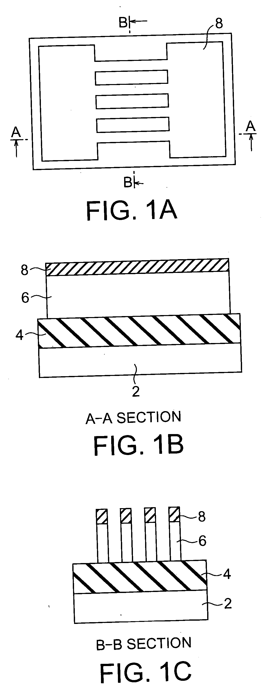
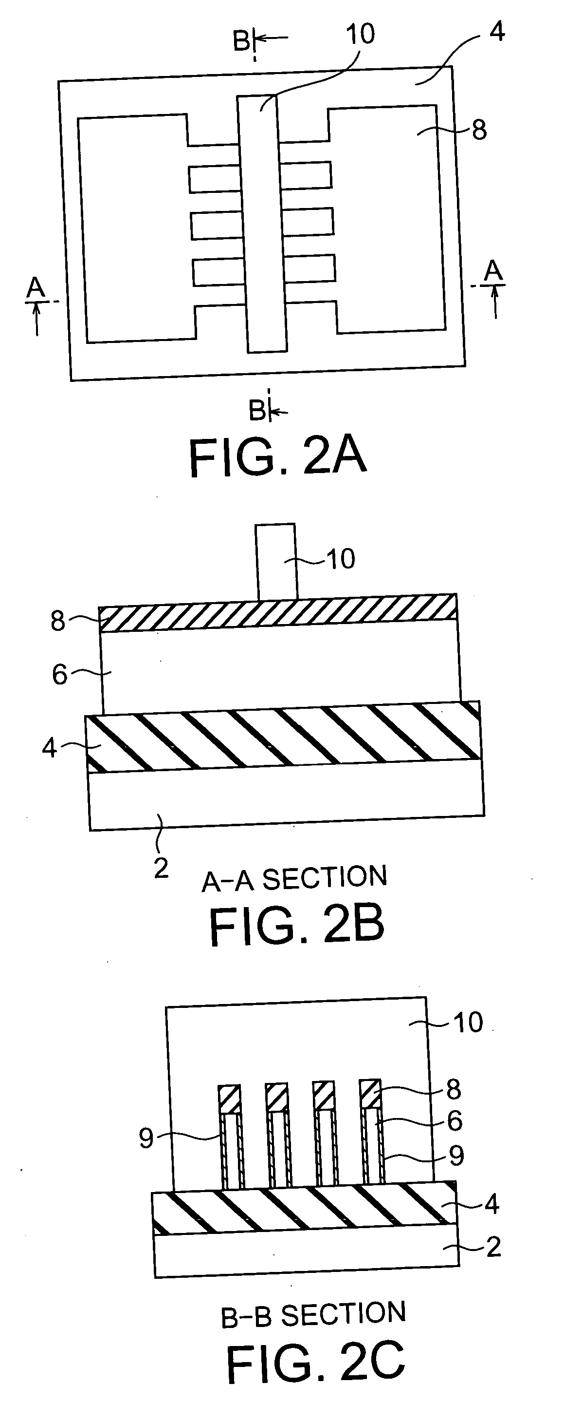
[0101] Next, the structure of a Fin-type channel transistor according to a first embodiment of the present invention will be described with reference to FIGS. 1A to 7. Although an n-type channel device will be described as an example of a Fin-type channel transistor according to this embodiment, a p-type channel device can also be manufactured in a similar manner by changing the kind of ion species implanted.

[0102] First, as shown in FIGS. 1A, 1B, and 1C, an SOI substrate is prepared by forming an insulating film 4 on a support substrate 2 and an SOI layer 6 on the insulating film 4. Thereafter, a silicon nitride layer 8 having a thickness of about 100 nm and serving as a protection layer of channels is deposited by LPCVD (Low Pressure Chemical Vapor Deposition) or the like, and device isolation is performed using a known device isolation technique. Subsequently, the SOI layer 6 is patterned using a known patterning technique, thereby forming Fins serving as chann...

second embodiment

(Second Embodiment)

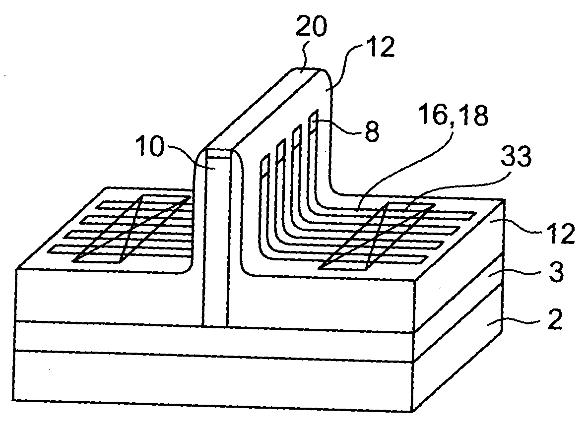
[0113] Next, FIGS. 8A to 10 show a structure of a Fin-type channel transistor according to a second embodiment of the present invention. FIG. 8A is a plan view of a Fin-type channel transistor according to this embodiment, FIG. 8B is a sectional view taken along line A-A of FIG. 8A, FIG. 8C is a sectional view taken along ling B-B of FIG. 8A, FIG. 9 is a sectional view taken along line C-C of FIG. 8A, and FIG. 10 is a perspective view of a Fin-type channel transistor according to this embodiment.

[0114] The Fin-type channel transistor according to this embodiment is formed on a bulk substrate, which differentiates the Fin-type channel transistor of this embodiment from the Fin-type channel transistor of the first embodiment formed on an SOI substrate. Although an n-type channel device will be described as an example of a Fin-type channel transistor of this embodiment, a p-type channel device can be manufactured in a similar manner.

[0115] A plurality of semiconduc...

third embodiment

(Third Embodiment)

[0122] Next, the structure of a Fin-type channel transistor according to a third embodiment of the present invention will be described with reference to FIGS. 11 and 12.

[0123] The Fin-type channel transistor of this embodiment is formed on a bulk silicon substrate, and includes an elevated source and drain layer 22 (FIG. 12). With such an elevated source and drain layer 22, the bottom area of the source and drain regions 16 can be decreased, thereby further decreasing the leakage current. Specifically, as shown in FIG. 11, the structure of this embodiment is similar to that of the second embodiment except for the existence of the source and drain regions 16 and the strip shape of the source and drain regions. After the state of FIG. 11, silicon epitaxial growth is performed to selectively cover the silicon-exposed portions 18 with the elevated silicon layer 22, as shown in FIG. 12. In FIG. 12, the elevated silicon layer 22 grows not only on the silicon-exposed por...


PUM


Abstract

It is possible to reliably implant an impurity into an impurity forming region, and to form a self-aligned silicides on the entire portion of the source and drain regions. There are provided: a first semiconductor layer of a first conductivity type in a substantially a rectangular solid shape formed on a substrate; a gate electrode formed on a pair of first side portions of the first semiconductor layer facing to each other with a gate insulating film being placed between the gate electrode and the first side portions; a second semiconductor layer of the first conductivity type connected to bottom portions of a pair of second side portions of the first semiconductor layer placed in a substantially perpendicular direction with respect to the first side portions, the second semiconductor layer extending along the substantially perpendicular direction; a first impurity region of a second conductivity type formed in the second semiconductor layer; second impurity regions formed on the pair of side portions of the first semiconductor layer and connected to the first impurity region; and a channel region formed between the second impurity regions of the first semiconductor layer.

Description

CROSS-REFERENCE TO RELATED APPLICATION [0001] This application is based upon and claims the benefit of priority from prior Japanese Patent Application Nos. 2005-92267 and 2006-27300, filed on Mar. 28, 2005 and Feb. 3, 2006, the entire contents of which are incorporated herein by reference. BACKGROUND OF THE INVENTION [0002] 1. Field of the Invention [0003] The present invention relates to a Fin-type channel transistor and a method of manufacturing the same. [0004] 2. Background Art [0005] In order to improve the performance of semiconductor integrated circuits, it is necessary to improve the performance of field effect transistors constituting each semiconductor integrated circuit. So far, the device performance has been improved by miniaturizing the devices. However, some point out the limitations of this method. Countermeasures to short channel effect and a decrease in parasitic resistance are considered to be serious problems. According to the International Semiconductor Roadmap,...

Claims


Application Information

Patent Timeline
IPC IPC(8): H01L21/8234H01L27/12H01L21/336H01L27/01H01L31/0392
CPCH01L21/823412H01L21/823437H01L21/84H01L27/088H01L29/78618H01L29/41733H01L29/66795H01L29/7848H01L29/785H01L27/1203
Inventor KINOSHITA, ATSUHIROKOGA, JUNJINAKABAYASHI, YUKIO
Owner KK TOSHIBA
Why Eureka
Try Eureka