
Semiconductor device and method for manufacturing same

Inactive Publication Date: 2006-10-05
KK TOSHIBA
View PDF6 Cites 53 Cited by
  • Summary
  • Abstract
  • Description
  • Claims
  • Application Information

AI Technical Summary

Benefits of technology

[0008] A semiconductor device according to one aspect of the present invention comprises: a first semiconductor layer of a first conductivity type; a pillar layer formed on the first semiconductor layer, the pillar layer comprising a first semiconductor pillar layer of a first conductivity type and a second semiconductor pillar layer of a second conductivity type which are alternately formed in a first direction along a surface of the first semiconductor layer; a first main electrode electrically connected to the first semiconductor layer; a semiconductor base layer of the second conductivity type selectively formed on a surface of the second semiconductor pillar layer; a semiconductor diffusion layer of the first conductivity type selectively formed on a surface of the semiconductor base layer; a second main electrode formed in contact with the semiconductor base layer and semiconductor diffusion layer; and a control electrode formed via an insulating film on the semiconductor base layer, semiconductor diffusion layer, and first semiconductor pillar layer, the semiconductor device further comprising a guard ring layer of the second conductivity type formed surrounding an outermost periphery of the semiconductor base layer, and the semiconductor base layer having a smaller junction depth than the guard ring layer.
[0009] A method for manufacturing a semiconductor device according to one aspect of the present invention comprises: forming on a first semiconductor layer of a first conductivity type a second semiconductor layer having a lower impurity concentration than the first semiconductor layer; forming a plurality of equally spaced trenches

Problems solved by technology

This may cause electric field concentration in that region, which can cause destruction of the device.
In the conventional device structures, therefore, the MOS gate structure cannot have a small cell pitch which is comparable to the small cell of the super junction structure, thereby providing an insufficiently low on-resistance.

Method used


Image

  • Semiconductor device and method for manufacturing same
  • Semiconductor device and method for manufacturing same
  • Semiconductor device and method for manufacturing same

Examples


first embodiment

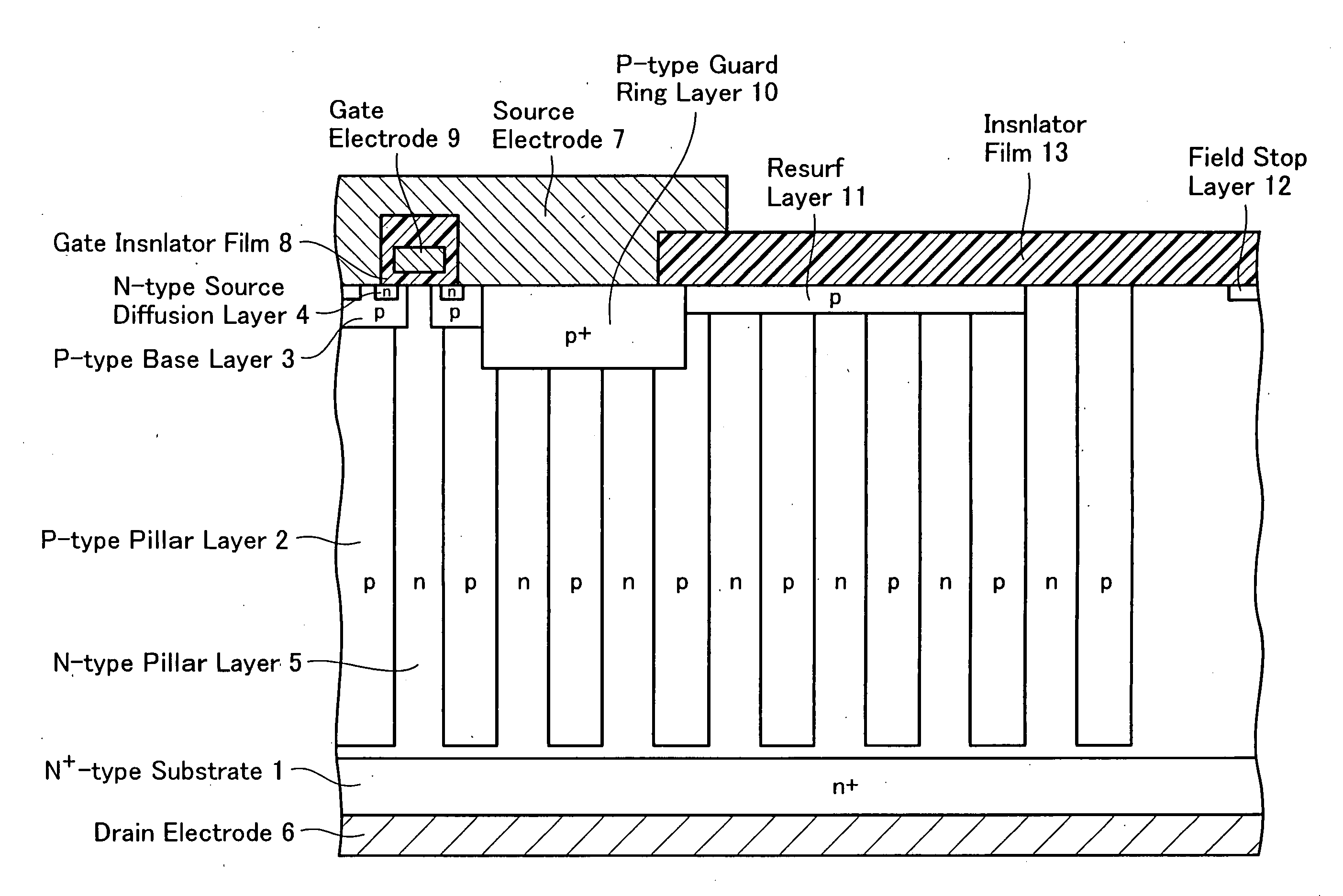
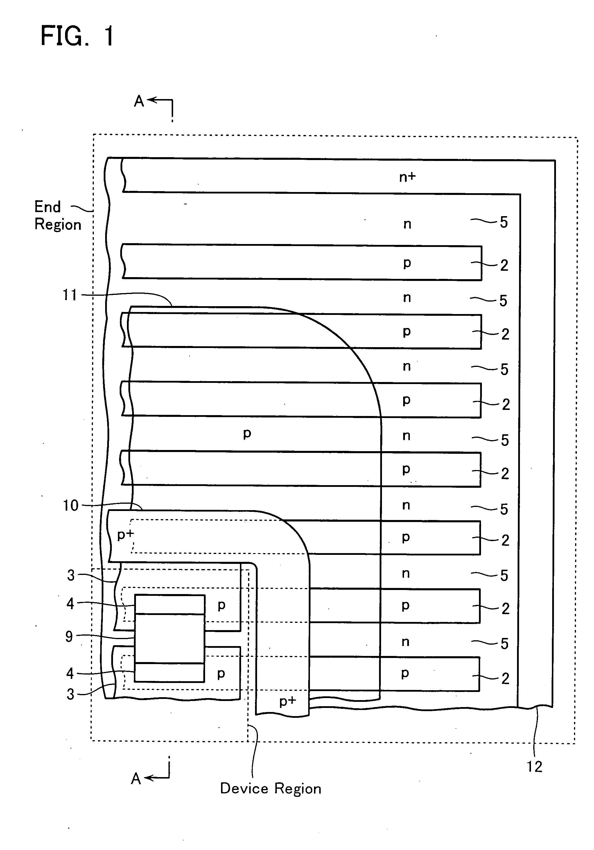
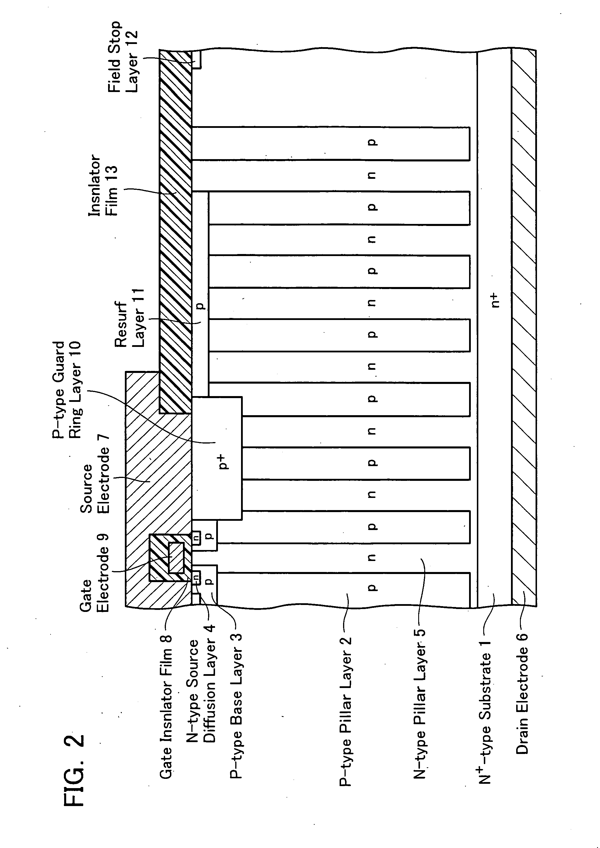
[0027]FIG. 1 is a schematic plan view of the configuration of the power MOSFET according to the first embodiment of the present invention. FIG. 2 is a cross sectional view along the line A-A in FIG. 2. The MOSFET has a super junction structure formed over the n+-type substrate 1 which functions as the drain layer. The super junction structure includes an n-type pillar layer 5 and a p-type pillar layer 2, which have a cross section of a vertically-oriented strip and are formed alternately in the lateral direction (the first direction) along the surface of the n+-type substrate 1. Formed under the n+-substrate 1 is a drain electrode 6 common to a plurality of MOSFETs. Note that although the example in FIG. 2 shows the p-type pillar layer 2 which is not contact with the n+-type substrate 1, the layer 2 can be configured to be in contact with the substrate 1.

[0028] A p-type base layer 3 in a stripe shape is selectively formed on the surface of the p-type pillar layer 2. An n-type sourc...

second embodiment

[0041]FIG. 9 is a schematic cross sectional view of the configuration of the power MOSFET according to the second embodiment of the present invention. The plan view is omitted here because it is substantially the same as FIG. 1 except for the resurf layer 11. In the power MOSFET according to this embodiment, an insulator film 13 resides on the surface of the super junction structure formed in the end region. A field plate electrode 14 resides on the insulator film 13, the field plate electrode 14 being connected to the source electrode 7. Consequently, as in the resurf structure in the first embodiment (FIG. 1), the depletion layer extends immediately laterally in the end region when the MOSFET is non-conducting, thereby helping to increase the breakdown voltage.

third embodiment

[0042]FIG. 10 is a schematic cross sectional view of the configuration of the power MOSFET according to the third embodiment of the present invention. This embodiment differs from the above embodiments in that the super junction structure is not formed in the end region, and alternatively, a high resistance layer 15 is formed, and a p-type guard ring layer 16 is formed on the high resistance layer 15. Also in this embodiment, when the MOSFET is non-conducting, the depletion layer extends laterally along the guard ring layer 16, thereby helping to increase the breakdown voltage.


PUM


Abstract

The present semiconductor device comprises pillar layers formed on a first semiconductor layer, the pillar layers comprising a first semiconductor pillar layer of a first conductivity type and a second semiconductor pillar layer of a second conductivity type which are alternately formed in a first direction along a surface of the first semiconductor layer. A semiconductor base layer of the second conductivity type is selectively formed on the surface of the second semiconductor pillar layer. A guard ring layer of the second conductivity type is formed surrounding the outermost periphery of the semiconductor base layer. The semiconductor base layer has a smaller junction depth than the guard ring layer.

Description

CROSS REFERENCE TO RELATED APPLICATIONS [0001] This application is based on and claims the benefit of priority from prior Japanese Patent Application No. 2005-97164, filed on Mar. 30, 2005, the entire contents of which are incorporated herein by reference. BACKGROUND OF THE INVENTION [0002] 1. Field of the Invention [0003] The present invention relates to a semiconductor device and a method for manufacturing the same. [0004] 2. Description of the Related Art [0005] The on-resistance of the vertical power MOSFET depends largely on the electrical resistance in the conduction layer (drift layer) portion. The electrical resistance of the drift layer depends on its impurity concentration. A higher impurity concentration can provide a lower on-resistance. A higher impurity concentration, however, will decrease the breakdown voltage of the PN junction between the drift layer and base layer. The impurity concentration thus cannot be higher than a limit determined by the breakdown voltage. A...

Claims


Application Information

Patent Timeline
IPC IPC(8): H01L29/76
CPCH01L29/0615H01L29/0619H01L29/0634H01L29/0696H01L29/7811H01L29/402H01L29/41741H01L29/66712H01L29/1095
Inventor SAITO, WATARUOMURA, ICHIRO
Owner KK TOSHIBA
Features
  • Generate Ideas
  • Intellectual Property
  • Life Sciences
  • Materials
  • Tech Scout
  • Unparalleled Data Quality
  • Higher Quality Content
  • 60% Fewer Hallucinations
Learn More