

Semiconductor device and method of manufacturing semiconductor device
- Summary
- Abstract
- Description
- Claims
- Application Information
AI Technical Summary
Benefits of technology
Problems solved by technology
Method used
Image

Examples
Embodiment Construction
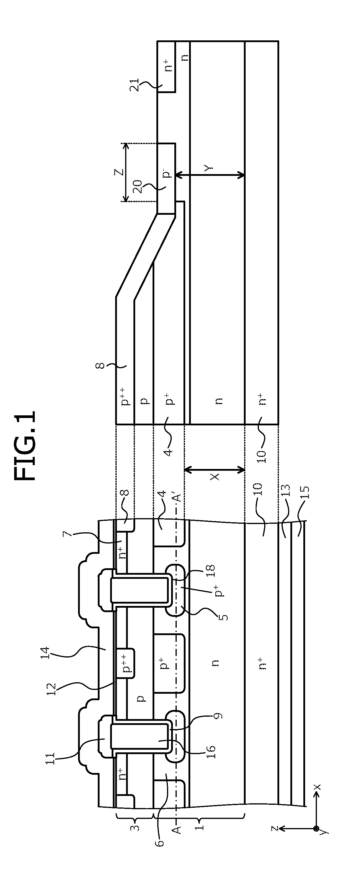
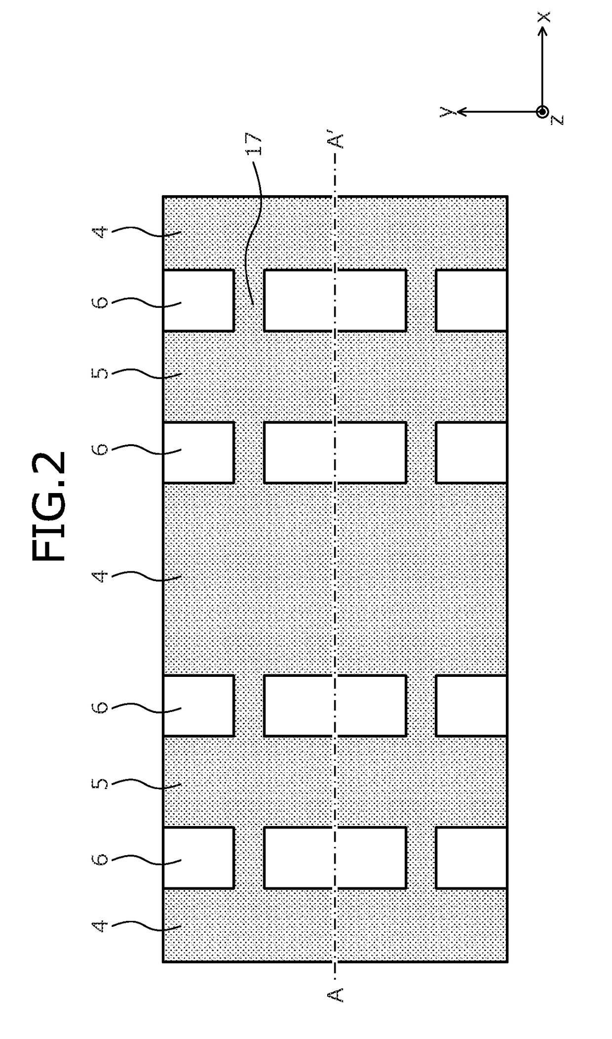
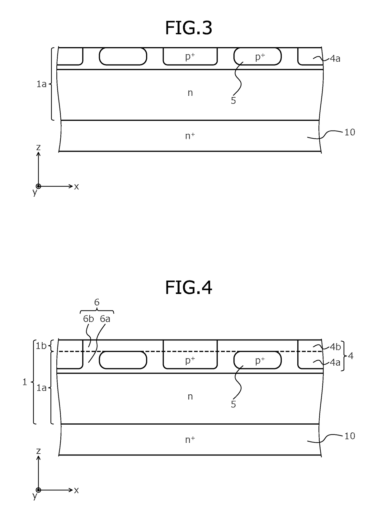
[0025]First, problems associated with the related arts will be described. When the technique described in Japanese Patent No. 5539931 is used and a pn junction is formed, manufacturing is extremely difficult because the breakdown voltage cannot be secured unless the pn junction is formed at a position deeper than the bottom of the trench or at a position near the trench. Further, when the technique described in U.S. Pat. No. 6,180,958 is used and a p-type region is formed, high electric field is likely to be applied to the gate insulating film at sidewalls of the trench and in an ON state, the current path narrows, increasing the ON resistance. Further, when the technique described in Japanese Laid-Open Patent Publication No. 2009-260253 is used and both a deep p-structure at a position separated from the trench and a p-type region at the bottom of the trench are formed, a width of a p-region at a lower part of the trench is made narrower than a width of the trench to reduce the ON ...
PUM
 Abstract
Description
Claims
Application Information