
Semiconductor integrated circuit

Active Publication Date: 2018-09-20
FUJI ELECTRIC CO LTD
View PDF0 Cites 1 Cited by
  • Summary
  • Abstract
  • Description
  • Claims
  • Application Information

AI Technical Summary

Benefits of technology

The patent text discusses the use of a device called an HVIC to transmit signals between different regions of a circuit. These regions can have different potentials, so they need to be electrically separated from each other. The text suggests that the most cost-effective way to do this is by using a self-isolation method that uses a pn-junction between a p-type diffusion region and an n-type diffusion region. This method is simple and effective, and can be used in the manufacturing process of the HVIC.

Problems solved by technology

When this current flows excessively into the circuit region, a malfunction of the circuit unit arranged in the circuit region may be induced.

Method used


Image

  • Semiconductor integrated circuit
  • Semiconductor integrated circuit
  • Semiconductor integrated circuit

Examples


first embodiment

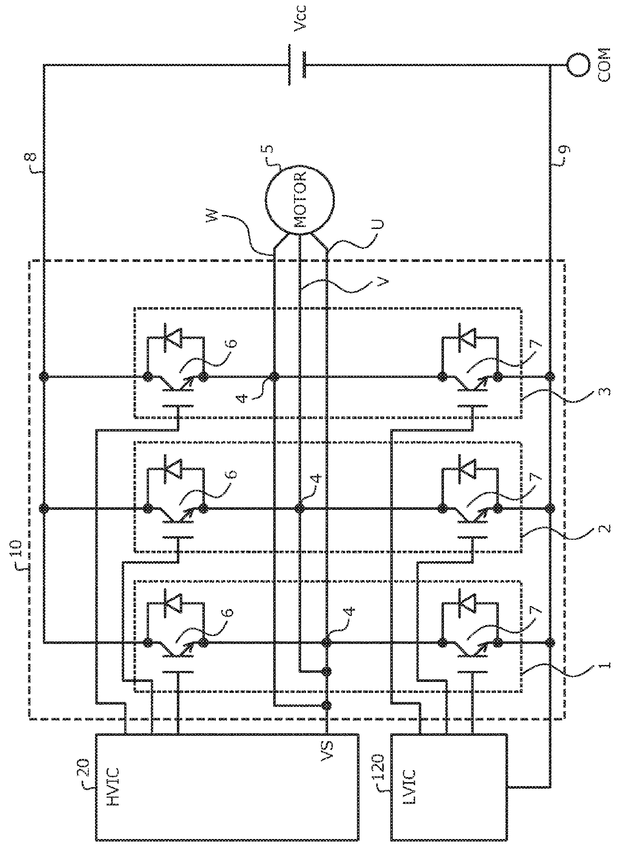
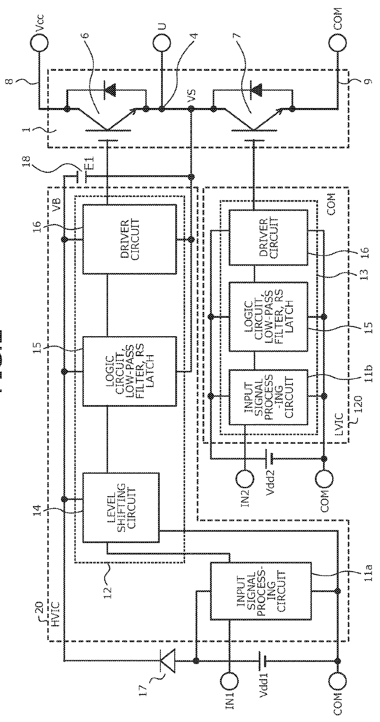
[0059]The connection point between the upper arm IGBT 6 and the lower arm IGBT 7 is the output point 4 of each of the half-bridge circuits 1 to 3, and is connected to a VS terminal of the high voltage integrated circuit (HVIC) 20. The HVIC 20 is a gate driver IC driving the IGBTs 6 in the upper arm constituting the three-phase inverter 10. The HVIC 20 is the semiconductor integrated circuit depicted in FIG. 3 described later. The potential of the VS terminal of the HVIC 20 varies between the power source potential Vcc of the three-phase inverter 10 and the common potential COM. A switching element such as a MOSFET may be used instead of each of the IGBTs 6 and 7. A low voltage integrated circuit (LVIC) 120 is a gate driver IC driving the IGBTs 7 in the lower arm that constitutes the three-phase inverter 10.

[0060]An example of a circuit configuration of the HVIC 20 will be described. FIG. 2 is a block diagram of the circuit configuration of an ordinary HVIC. FIG. 2 depicts the half-...

fifth embodiment

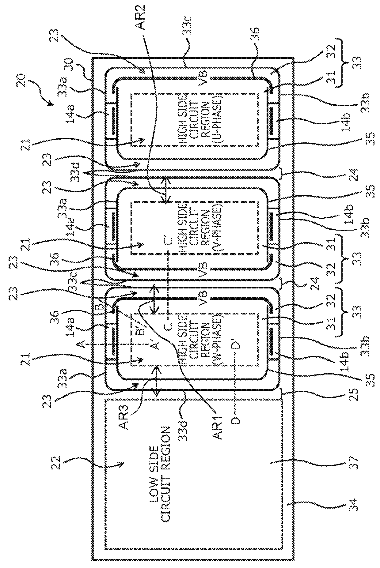
[0111]The distance is thereby reduced on the front surface of the semiconductor substrate 30 between the PG circuit and the HVNMOSs 14a and 14b. Gate wires of the HVNMOSs 14a and 14b, and the like, therefore, do not need to be run on the semiconductor substrate 30 from the n-type well region 33 in which the HVNMOSs 14a and 14b are arranged to a point separated therefrom, and the variation of the gate driving performance of each of the phases may be reduced. Occurrences of malfunctions such as self-turning on caused by fluctuation of the gate voltage (a phenomenon that the HVNMOSs 14a and 14b are errantly turned on due to an increase of the gate voltages) may be suppressed. The arrangement and the circuit configuration of the input signal processing circuit 11a of the HVIC 20 depicted in FIG. 13 will be described in the fifth embodiment described later.

[0112]The HVIC 20 depicted in FIG. 14 includes fewer high side circuit regions 21 than the HVIC 20 of the first embodiment (see FIG. ...


PUM


Abstract

A semiconductor integrated circuit includes semiconductor substrate having a plurality of first potential side areas, including a first two adjacent first potential side areas, each first potential side area having a high potential side circuit, a first semiconductor region of a first conductivity type selectively provided in a surface layer on a front surface of a semiconductor substrate, a second semiconductor region of a second conductivity type selectively provided in the first semiconductor region, penetrating the first semiconductor region in a depth direction, a third semiconductor region of the first conductivity type selectively provided in the first semiconductor region so as to be separated from the second semiconductor region. Each of the first two adjacent first potential side areas includes a first side area facing the other, each first side area includes the third semiconductor region, and is free of the second semiconductor region.

Description

CROSS REFERENCE TO RELATED APPLICATIONS[0001]This application is based upon and claims the benefit of priority of the prior Japanese Patent Application No. 2017-053178, filed on Mar. 17, 2017, the entire contents of which are incorporated herein by reference.BACKGROUND OF THE INVENTION1. Field of the Invention[0002]Embodiments of the present invention relate to a semiconductor integrated circuit.2. Description of the Related Art[0003]For a high voltage integrated circuit (HVIC), a conventionally known separation method uses a high voltage junction that electrically separates a high potential side (a high side) circuit region and a low potential side (a low side) circuit region provided on a single semiconductor substrate (a semiconductor chip) from each other using a high voltage junction termination region (HVJT) provided between these circuit regions.[0004]The HVIC has a function of converting an input signal using, as a benchmark, the ground potential (the ground) GND that is a r...

Claims


Application Information

Patent Timeline
IPC IPC(8): H01L27/092H01L27/06H01L29/417H01L29/866
CPCH01L27/0922H01L27/0623H01L27/0928H01L29/41766H01L29/866H01L21/761H01L21/823892H02M7/5387H01L29/7816H01L29/78
Inventor TANAKA, TAKAHIDE
Owner FUJI ELECTRIC CO LTD
Features
  • Generate Ideas
  • Intellectual Property
  • Life Sciences
  • Materials
  • Tech Scout
  • Unparalleled Data Quality
  • Higher Quality Content
  • 60% Fewer Hallucinations
Learn More