Structure of a structure release and a method for manufacturing the same

a technology of structure release and manufacturing method, which is applied in the direction of static indicating devices, instruments, non-linear optics, etc., can solve the problems of poor capacity for lateral etching, high cost and instability of etchant xenon difluoride, and prolong the life cycle of the remote plasma, so as to reduce the time taken, the effect of efficient structure release etching of the sacrificial layer

Inactive Publication Date: 2006-10-05
SNAPTRACK
View PDF0 Cites 101 Cited by
  • Summary
  • Abstract
  • Description
  • Claims
  • Application Information

AI Technical Summary

Benefits of technology

[0025] In addition, the present invention preferably uses remote plasma. A plasma is first produced in a plasma generator, and after portion or all of the charged composition in the plasma is filtered out, the remaining plasma, the remote plasma, is sent into a chamber to perform a reaction. Free radicals are the main composition of the remote plasma, so a life cycle of the remote plasma is longer and the structure release etching of the sacrificial layer is performed efficiently. Besides, the free radicals are not charged and not easily affected by an electric field, so the effect of isotropic etching is better for being beneficial to lateral etching.
[0026] According to the optical interference display cell structure and the method for manufacturing the same of the present invention, the holes in the second electrode can indeed reduce the time taken in the structure release etching, to make it possible for a conventional etching process to replace a xenon difluoride etching process, and to avoid the difficulties resulting from reorganizing and consolidating the process apparatuses. The use of the remote plasma increases the lift cycle of the etching plasma and the lateral etching capacity of the plasma, accelerates the rate of the structure release etching, decrease the time needed in the structure release etching, and increases the throughput of the optical interference display.

Problems solved by technology

The development of the etching apparatus with an etchant of xenon difluoride is not maturing, which is disadvantageous to the development and throughput of the optical interference display, and the etchant xenon difluoride is expensive and unstable.
The reason that the etching apparatus used in typical semiconductor or planar display is not suitable for use in the structure release etching process is the poor capacity for lateral etching, and even though an etchant with a great etching property, for example, nitrogen trifluoride (NF3) or sulphur hexafluoride (SF6), is used, the etching rate is only between 3 micrometers and 10 micrometers per minute.
This is slower than that for using xenon difluoride as an etchant by several to dozens of times. Therefore, this is very disadvantageous to throughput of the optical interference display.

Method used


Image

  • Structure of a structure release and a method for manufacturing the same
  • Structure of a structure release and a method for manufacturing the same
  • Structure of a structure release and a method for manufacturing the same

Examples


Embodiment Construction

[0036] In order to make the illustration of a structure of a structure release and a method for manufacturing the same provided in the present invention more clear, an embodiment of the present invention herein takes an optical interference display cell structure and a manufacturing method thereof for example, to illustrate how to apply the structure of the structure release and the method for manufacturing the same disclosed in the present invention, and to further explain advantages of the present invention according to the disclosure of the embodiment.

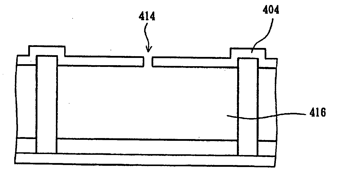
[0037]FIG. 5 illustrates a top view of an optical interference display cell in accordance with a preferred embodiment of the present invention. Referring to FIG. 5, an optical interference display cell 300 includes an electrode 301, separation structures 302, such as defined by a dotted line 3021, and supporters 304. The separation structures 302 are located on two opposite sides of the optical interference display cell 300. The su...


PUM

PropertyMeasurementUnit
diameteraaaaaaaaaa
diameteraaaaaaaaaa
diameteraaaaaaaaaa

Abstract

A structure of a structure release and a manufacturing method are provided. The structure and manufacturing method are adapted for an interference display cell. The structure of the interference display cell includes a first electrode, a second electrode and at least one supporter. The second electrode has at least one hole and is arranged about parallel with the first electrode. The supporter is located between the first electrode and the second electrode and a cavity is formed. In the release etch process of manufacturing the structure, an etchant can pass through the hole to etch a sacrificial layer between the first and the second electrodes to form the cavity; therefore, the time needed for the process becomes shorter.

Description

CROSS-REFERENCE TO RELATED APPLICATIONS [0001] This application is a continuation-in-part, and hereby incorporates by reference the entire disclosure, of U.S. patent application Ser. No. 10 / 644,312, filed Aug. 19, 2003. [0002] Moreover, this application incorporates by reference U.S. patent application Ser. No. 11 / 090,911, filed Mar. 25, 2005; U.S. patent application Ser. No. 11 / 150,496, filed Jun. 10, 2005; U.S. Pat. No. 5,835,255, issued Nov. 10, 1998; U.S. Pat. No. 5,986,796, issued Nov. 16, 1999; U.S. Pat. No. 6,040,937, issued Mar. 21, 2000; U.S. Pat. No. 6,055,090, issued Apr. 25, 2000; U.S. Pat. No. 6,650,455, issued Nov. 18, 2003; U.S. Pat. No. 6,674,562, issued Jan. 6, 2004; U.S. Pat. No. 6,741,377, issued May 25, 2004; and U.S. Pat. No. 6,870,654, issued Mar. 22, 2005.BACKGROUND OF THE INVENTION [0003] 1. Field of the Invention [0004] The present invention relates to a structure of a structure release and a method for manufacturing the same, and more particularly, the pres...

Claims


Application Information

Patent Timeline
Patent Type & Authority Applications(United States)
IPC IPC(8): H01L29/84H01L21/00H01L33/00H01L31/12H01L27/15H01L29/26G01J3/26G02B6/12G02B26/00G02B26/02G02B26/08G02F1/137G02F1/21G09G3/34
CPCB82Y20/00G01J3/26G02B6/12G02B26/001G09G3/3466G02F1/13725G02F1/216G02F2203/03G02B2006/12104G02B26/00
Inventor MILES, MARK W.
Owner SNAPTRACK
Why Eureka
Try Eureka