Multi-chip package and method for manufacturing the same

Inactive Publication Date: 2006-10-05
SAMSUNG ELECTRONICS CO LTD
View PDF14 Cites 15 Cited by
  • Summary
  • Abstract
  • Description
  • Claims
  • Application Information

AI Technical Summary

Benefits of technology

[0016] An example embodiment of the present invention provides a multi-chip package with improved overall production rates.

Problems solved by technology

If the upper semiconductor chip of adjacent semiconductor chips is equal or larger in size than the lower semiconductor chip of adjacent semiconductor chips, the bonding wires of the lower semiconductor chip may contact the upper semiconductor chip, causing a short circuit.
The conventional multi-chip package 100 may have negative impact on production rates.
Faulty chips can dramatically impact production rates because a single faulty chip among the semiconductor chips 20, 30 and 40 will cause failure of the entire multi-chip package 100.
Therefore, the semiconductor chips 20, 30 and 40 are sometimes tested at chip level, e.g., prior to packaging, but such more sophisticated chip-level testing techniques may result in increased overall production costs.
In particular, if a multi-chip package includes memory chips and application specific integrated circuits (ASICs), for example logic chips, the multi-chip package may bear an excess burden of production costs, especially when the less expensive and more failure-prone memory chips cause failure of an entire multi-chip package containing otherwise viable logic chips.
Generally, the memory chips may show higher fault rates than the logic chips.
This may cause faulty multi-chip packages.
If the multi-chip packages are tested using a testing process for memory chips, logic chips that would have been passed under typical test conditions for logic chips, may be determined to be faulty.
As a result, failure of relatively less expensive and more failure-prone chips, e.g., memory chips, does not waste viable and more expensive chips, e.g., logic chips.

Method used


Image

  • Multi-chip package and method for manufacturing the same
  • Multi-chip package and method for manufacturing the same
  • Multi-chip package and method for manufacturing the same

Examples


Embodiment Construction

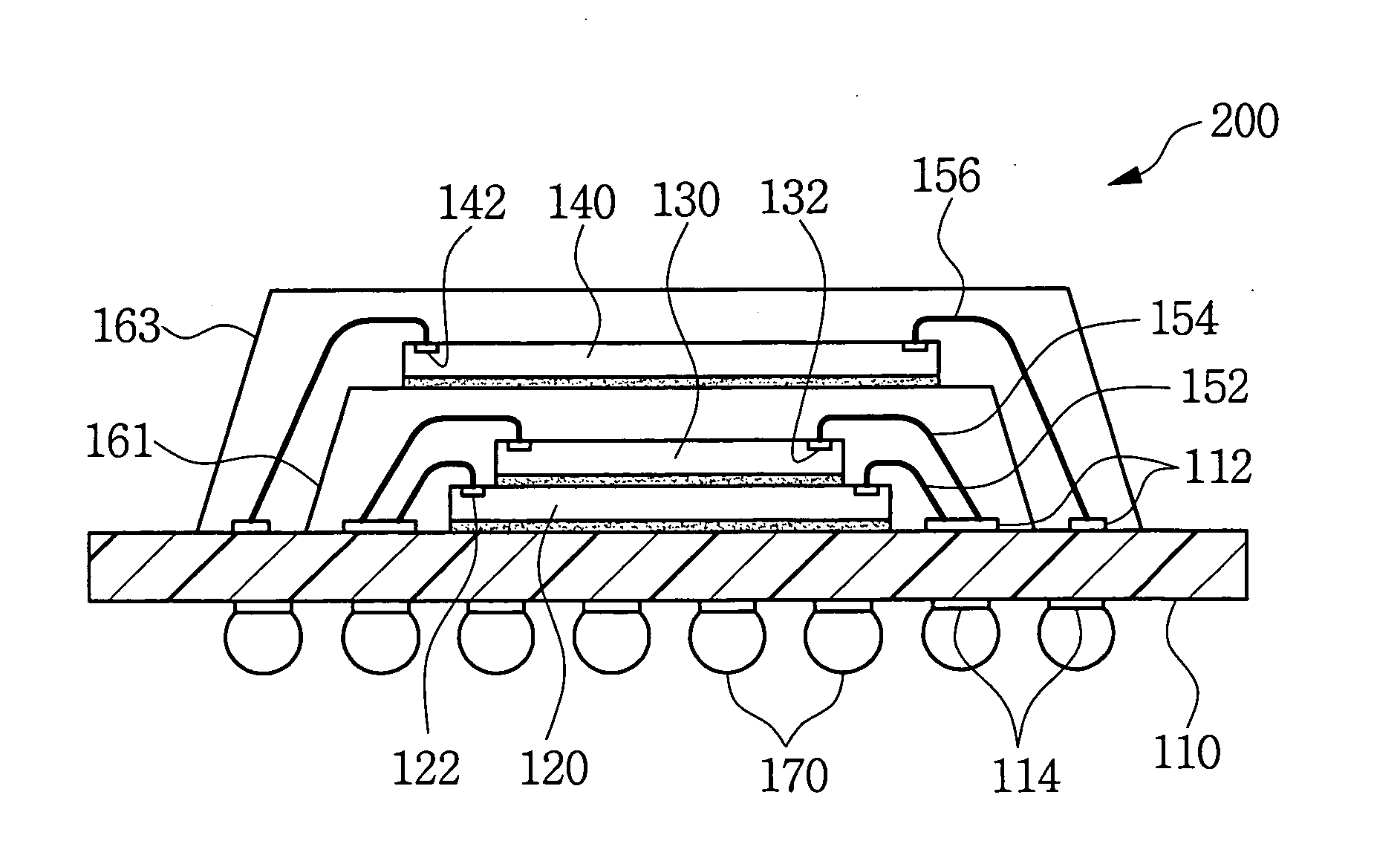
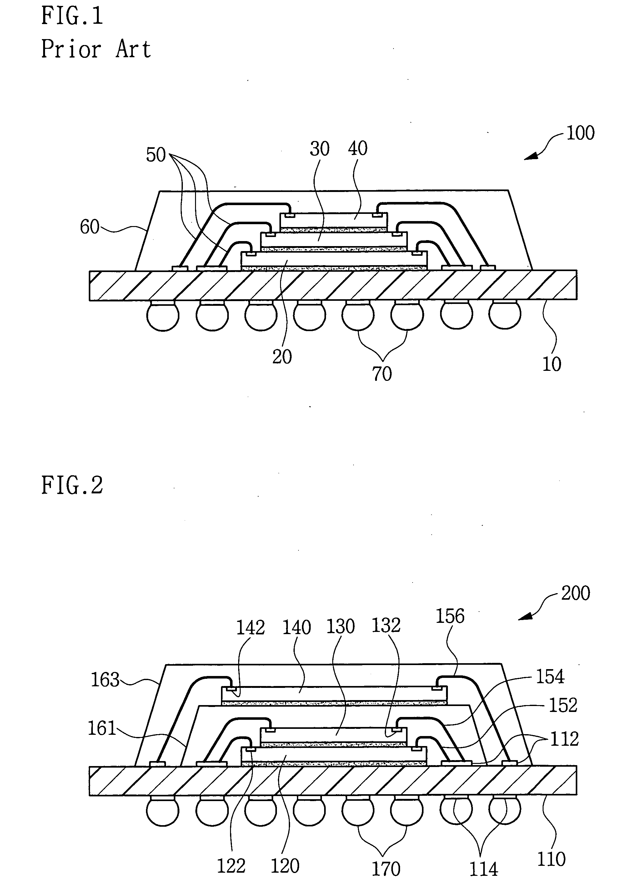
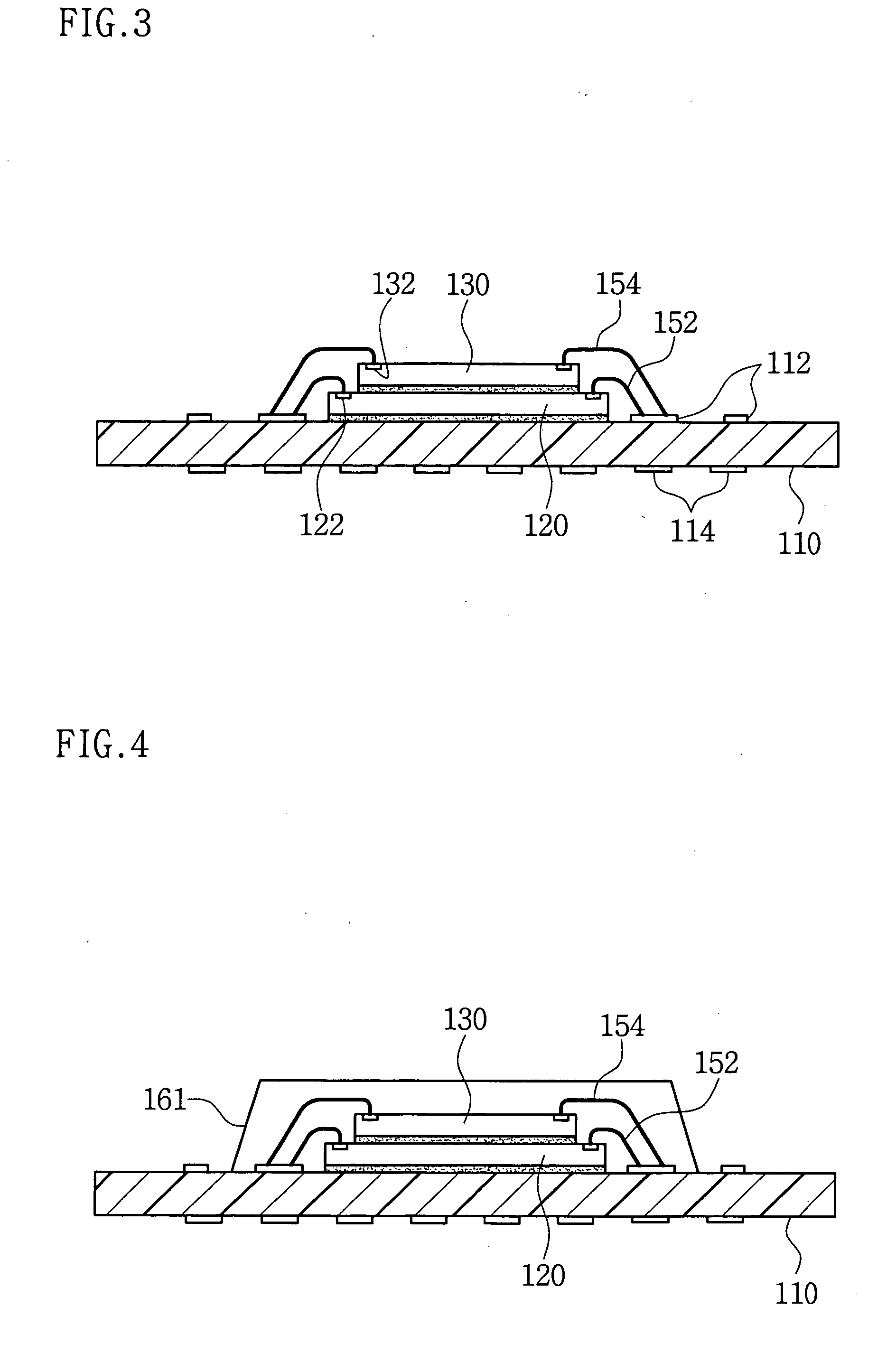
[0042] Example, non-limiting embodiments of the present invention will now be described more fully with reference to the accompanying drawings. This invention may, however, be embodied in many different forms and should not be construed as limited to the particular example embodiments set forth herein. Rather, the disclosed embodiments are provided as illustrative disclosure, and will convey the invention to those skilled in the art. The principles and features of this invention, therefore, may be employed in varied and numerous embodiments without departing from the scope of the invention.

[0043] It should be noted that the figures are intended to illustrate the general characteristics of methods and devices of example embodiments of this invention and for the purpose of the description of such example embodiments herein. These drawings are not, however, to scale and may not precisely reflect the characteristics of any given embodiment, and should not be interpreted as defining or ...


PUM


Abstract

A multi-chip package includes a first chip group including at least one semiconductor chip on a substrate. The first chip group may be sealed to form a first package body. Connecting test terminals to ball pads allows package-level testing of the first chip group. A second chip group including at least one semiconductor chip may be provided on the first package body. The first package body and the second chip group may be sealed to form a second package body. The multi-chip package may further comprise an interposer substrate provided between the first package body and, for example, the lowest semiconductor chip of the second chip group. The interposer substrate may electrically connect the second chip group to the substrate.

Description

CROSS REFERENCE TO RELATED APPLICATIONS [0001] This U.S. non-provisional application claims benefit of priority under 35 U.S.C. §119 of Korean Patent Application No. 2005-23112, filed on Mar. 21, 2005, the entire contents of which are incorporated herein by reference. BACKGROUND OF THE INVENTION [0002] 1. Field of the Invention [0003] The present invention relates to a semiconductor packaging technique, and more particularly, to a multi-chip package and a method for manufacturing the same. [0004] 2. Description of the Related Art [0005] Demands continue for semiconductor products that are lighter, smaller and thinner, and include multiple semiconductor chips. To meet such demands, multi-chip semiconductor packages have been developed. [0006] Multi-chip semiconductor packages may include at least two semiconductor chips in a single semiconductor package. The semiconductor chips may be the same or different kinds of semiconductor chips. The semiconductor chips may be vertically or hor...

Claims


Application Information

Patent Timeline
IPC IPC(8): H01L23/52
CPCH01L23/3128H01L23/3135H01L2224/32245H01L24/48H01L2924/15311H01L2924/1433H01L2924/01079H01L2225/06582H01L2225/06579H01L2225/06572H01L2225/06568H01L2225/06558H01L23/4951H01L25/0652H01L25/0657H01L25/105H01L25/18H01L25/50H01L2224/16145H01L2224/16225H01L2224/32145H01L2224/48091H01L2224/48095H01L2224/48225H01L2224/48247H01L2224/73265H01L2225/0651H01L2924/00014H01L2924/00H01L2224/48227H01L2224/32225H01L2224/73253H01L2924/19107H01L2924/181H01L24/73H01L2924/14H01L2924/00012H01L2224/45099H01L2224/45015H01L2924/207H04M1/0216
Inventor LEE, DAE-HO
Owner SAMSUNG ELECTRONICS CO LTD
Why Eureka
Try Eureka