Compensating for coupling in non-volatile storage

Active Publication Date: 2006-10-05
SANDISK TECH LLC
View PDF32 Cites 48 Cited by
  • Summary
  • Abstract
  • Description
  • Claims
  • Application Information

AI Technical Summary

Benefits of technology

[0019] Some embodiments include programming a first set of non-volatile storage elements and a second set of non-volatile storage elements, both of which store first and second groupings of data. The programming includes writing to a particular non-volatile storage element with respect to the second grouping of data subsequent to writing to adjacent non-volatile storage elements for the first grouping of data. When intending to read data from the first set of non-volatile storage elements, the system will also read from the second set of non-volatile storage elements. The reading from the second set of non-volatile storage elements does not require reading accurate data, rather the read

Problems solved by technology

The coupling from adjacent memory cells can shift the apparent charge level being read a sufficient amount to lead to an erroneous reading of the data stored.

Method used


Image

  • Compensating for coupling in non-volatile storage
  • Compensating for coupling in non-volatile storage
  • Compensating for coupling in non-volatile storage

Examples


Embodiment Construction

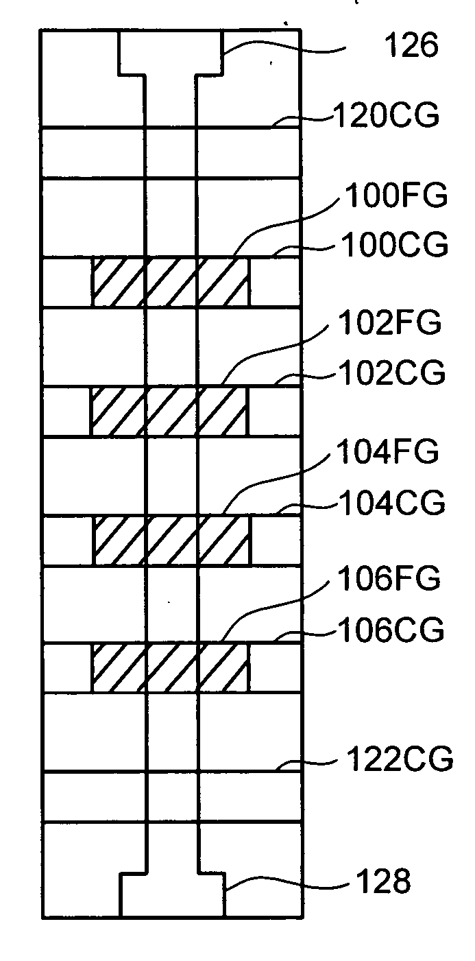
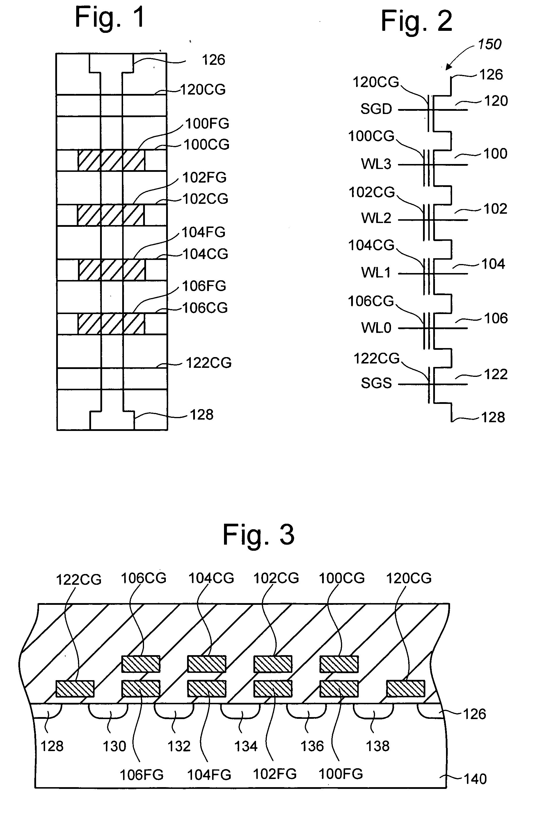
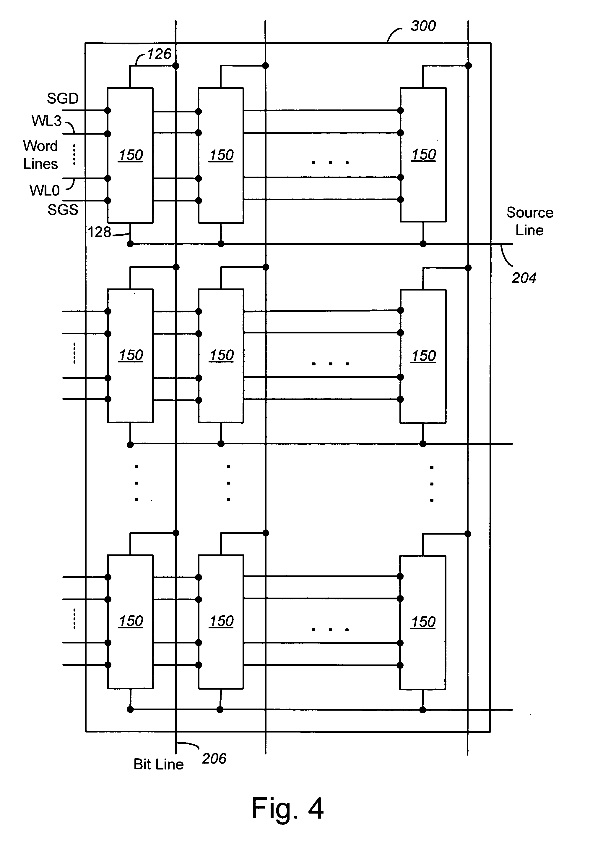
[0057] One example of a memory system suitable for implementing the present invention uses the NAND flash memory structure, which includes arranging multiple transistors in series between two select gates. The transistors in series and the select gates are referred to as a NAND string. FIG. 1 is a top view showing one NAND string. FIG. 2 is an equivalent circuit thereof. The NAND string depicted in FIGS. 1 and 2 includes four transistors, 100, 102, 104 and 106, in series and sandwiched between a first select gate 120 and a second select gate 122. Select gate 120 connects the NAND string to bit line 126. Select gate 122 connects the NAND string to source line 128. Select gate 120 is controlled by applying the appropriate voltages to control gate 120CG. Select gate 122 is controlled by applying the appropriate voltages to control gate 122CG. Each of the transistors 100, 102, 104 and 106 has a control gate and a floating gate. Transistor 100 has control gate 100CG and floating gate 100...


PUM


Abstract

Shifts in the apparent charge stored on a floating gate (or other charge storing element) of a non-volatile memory cell can occur because of the coupling of an electric field based on the charge stored in adjacent floating gates (or other adjacent charge storing elements). The problem occurs most pronouncedly between sets of adjacent memory cells that have been programmed at different times. To compensate for this coupling, the read process for a given memory cell will take into account the programmed state of an adjacent memory cell.

Description

CROSS-REFERENCE TO RELATED APPLICATIONS [0001] This Application is related to U.S. patent application titled “Compensating For Coupling During Read Operations Of Non-Volatile Memory,” by Jian Chen, Attorney Docket No. SAND-01040US0, filed on the same day as the present application, which is incorporated herein by reference in its entirety. [0002] This Application is related to U.S. patent application titled “Read Operation For Non-Volatile Storage That Includes Compensation For Coupling,” by Yan Li and Jian Chen, Attorney Docket No. SAND-01045US0, filed on the same day as the present application, which is incorporated herein by reference in its entirety.BACKGROUND OF THE INVENTION [0003] 1. Field of the Invention [0004] The present invention relates to technology for non-volatile memory. [0005] 2. Description of the Related Art [0006] Semiconductor memory has become more popular for use in various electronic devices. For example, non-volatile semiconductor memory is used in cellular...

Claims


Application Information

Patent Timeline
IPC IPC(8): G11C16/04
CPCG11C11/5628G11C11/5642G11C16/3431G11C16/3418G11C16/3422G11C16/26G11C16/34
Inventor CHEN, JIANCERNEA, RAUL-ADRIANHEMINK, GERRIT JAN
Owner SANDISK TECH LLC
Why Eureka
Try Eureka