Non-volatile memory electronic device with NAND structure being monolithically integrated on semiconductor

Active Publication Date: 2006-10-12
MICRON TECH INC
View PDF4 Cites 15 Cited by
  • Summary
  • Abstract
  • Description
  • Claims
  • Application Information

AI Technical Summary

Benefits of technology

[0028] A further object of the present invention is that of providing a type of memory electronic device wherein the two portions of memory matrix having different data storage capacity and different access speed can exploit the same structural sources but can be decoupled accord

Problems solved by technology

However, although having the feature of a superior data modify speed, such NAND memories do not allow a fast random access to the same, since they are oriented to readings of entire pages of at least 512 bytes, but not of the single bytes.
In fact, the NAND access protocol is quite slow in random access due to the known latency time, and it exhibits serious difficulties for acceding into a sector or a page in a random way.
Secondly, the costs of the resulting package cannot differ significantly from the global cost of the various components, since they cannot exploit large scale economies in the realization of devices assembled with components being different from one another.
There exist, then, a series of problems to be faced starting from the assumption that only a detailed comprehension of the phenomena apt to the memorization of the data inside the memory cells can allow understanding of the intrinsic limits of the adopted technology.
This field suffers from the length of the memory cell arrays which require high propagation times in the reading step for allowing reaching the cells being farthest from the node to which the reading potential is applied.
Moreover, it is also to be noted that the lithographi

Method used


Image

  • Non-volatile memory electronic device with NAND structure being monolithically integrated on semiconductor
  • Non-volatile memory electronic device with NAND structure being monolithically integrated on semiconductor
  • Non-volatile memory electronic device with NAND structure being monolithically integrated on semiconductor

Examples


Embodiment Construction

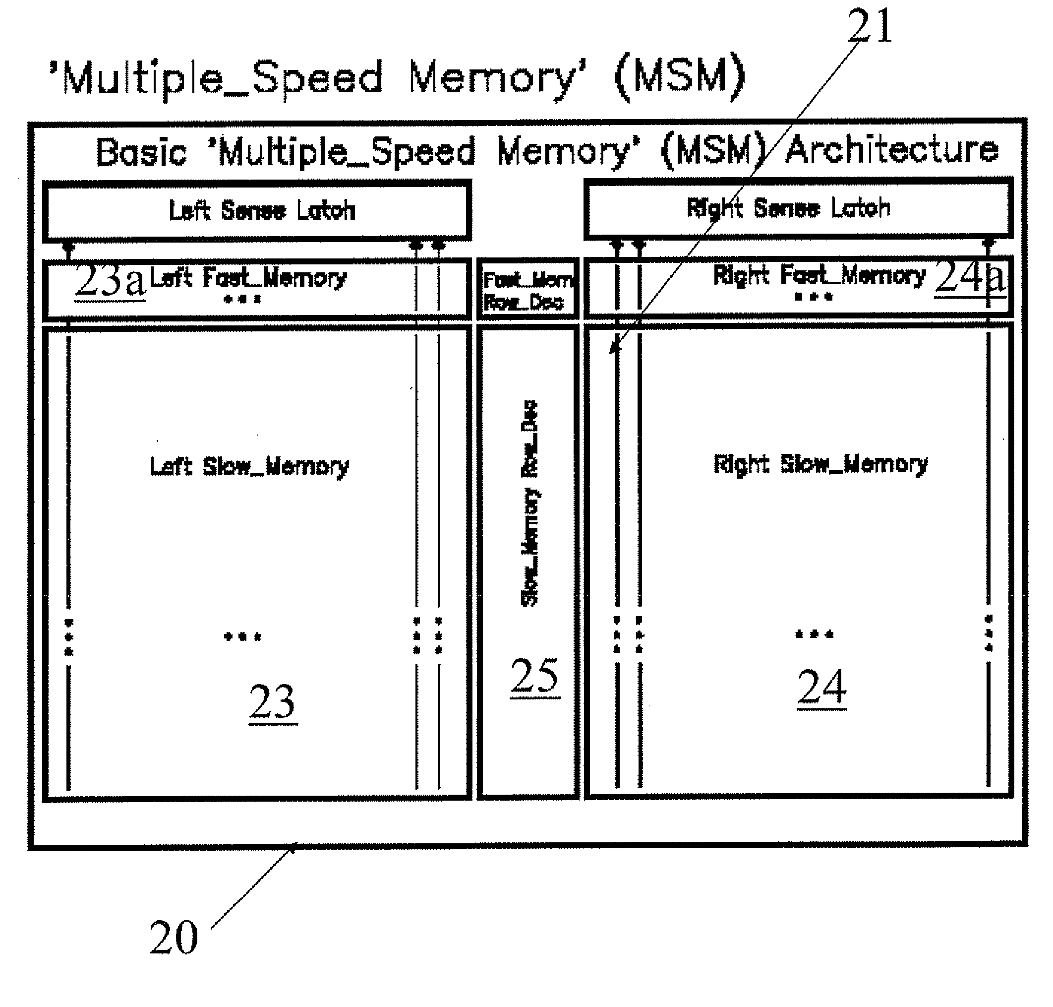
[0059] With reference to the figures, and in particular to the example of FIG. 2, a new memory electronic device realized according to the present invention and monolithically integrated on semiconductor is globally and schematically indicates at 20.

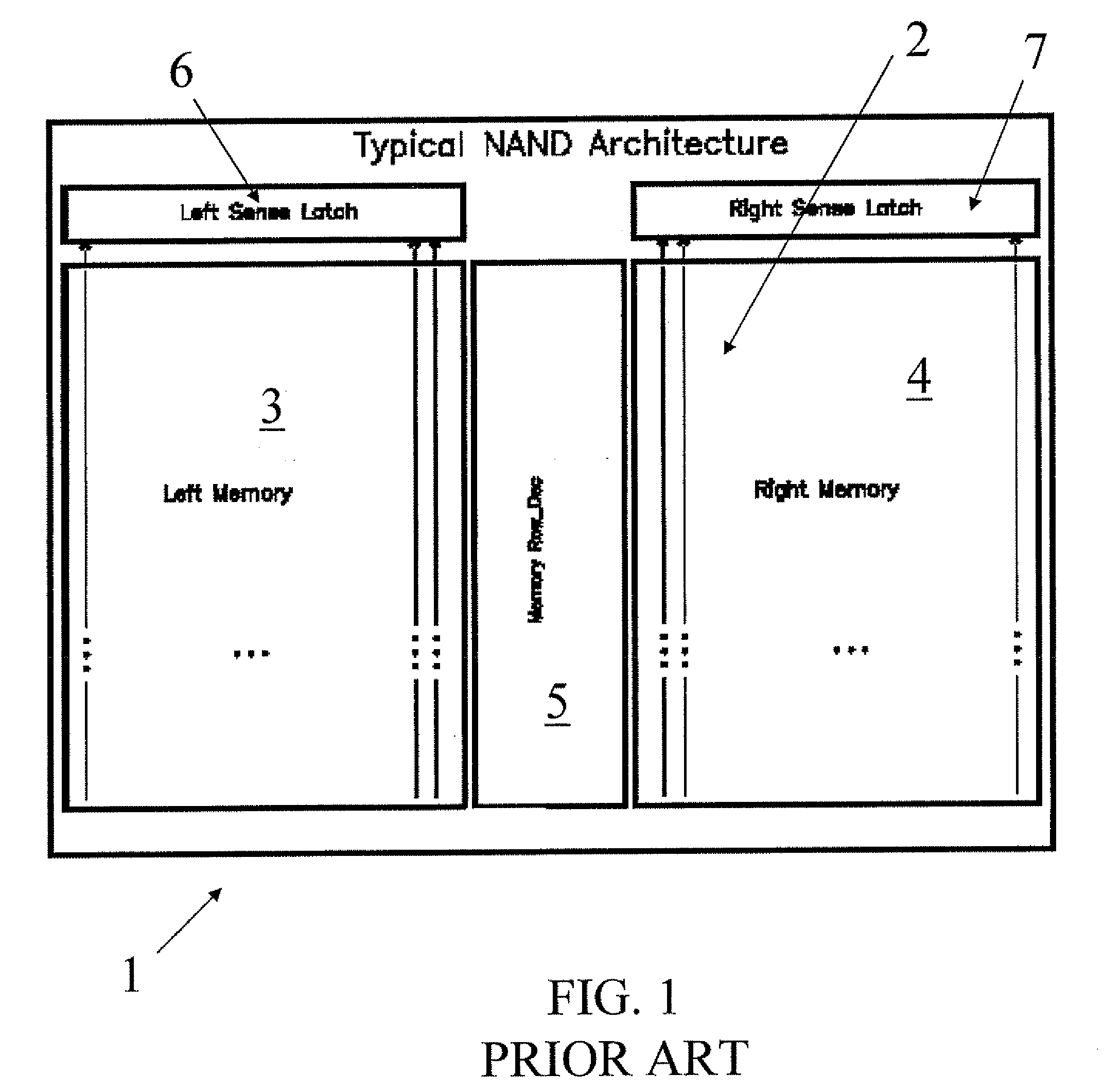
[0060] The device 20 incorporates at least one matrix 21 of memory cells organized in rows or word lines WL and columns or bit lines BL. In the embodiment here described by way of non-limiting example, the device 20 is a memory of the Flash EEPROM type with an architecture of the NAND type. However, nothing forbids that the principles described herein to be applied to a Flash NOR memory, or to an EPROM, or even to a Flotox EEPROM.

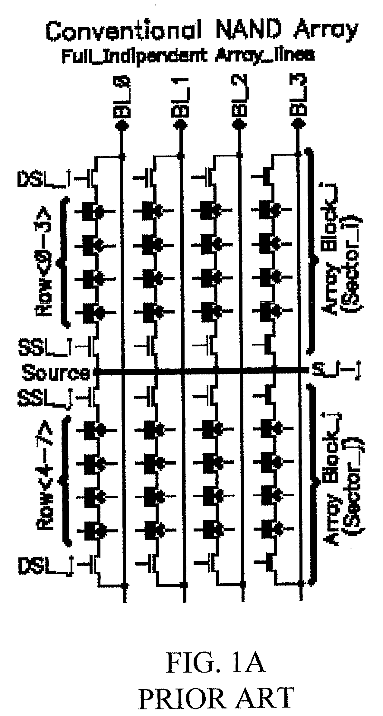
[0061] The only particularity is given by the fact that the memory matrix has a Bit Line which is common to more physical sectors of the matrix; in particular such Bit Line can be a MAIN Bit Line, as schematically shown in FIG. 4A, which is locally decoded in LOCAL Bit Lines for acceding to the memory cells of...


PUM

PropertyMeasurementUnit
Weightaaaaaaaaaa
Electrical conductivityaaaaaaaaaa
Structureaaaaaaaaaa

Abstract

A non-volatile memory electronic device is integrated on a semiconductor with an architecture including at least one memory matrix organized in rows or word lines and columns or bit lines of memory cells. The matrix is divided into at least a first and a second memory portions having a different access speed. The first and second memory portions may share the structures of the bit lines which correspond to one another and one by one and are electrically interrupted by controlled switches placed between the first and the second portions.

Description

FIELD OF THE INVENTION [0001] The present invention relates to a Flash EEPROM electronic memory device monolithically integrated on semiconductor and having a NAND architecture comprising at least one memory matrix organized in memory cell rows and columns. The invention also relates to a method for programming the above memory device with the NAND structure. BACKGROUND OF THE INVENTION [0002] It is known that the market for non-volatile memories, for example of the EEPROM or Flash EEPROM type, is currently growing significantly and the most promising applications relate to the “data storage” field. Until a few years ago, such a market almost exclusively involved the consumer field of digital cameras, with the associated memory cards, or the known USB keys which represented expansion mobile memories for personal computers. Therefore, the demand for these products by the consumer market was mainly addressed to flash memories of large capacity. [0003] This trend seems to be destined t...

Claims


Application Information

Patent Timeline
IPC IPC(8): G11C16/04
CPCG11C16/0483G11C16/12Y10T29/49002G11C16/08G11C16/24G11C16/0408
Inventor PASCUCCI, LUIGIROLANDI, PAOLO
Owner MICRON TECH INC
Why Eureka
Try Eureka