Surface emitting semiconductor laser array and optical transmission system using the same

Active Publication Date: 2006-10-12
FUJIFILM BUSINESS INNOVATION CORP
View PDF4 Cites 52 Cited by
  • Summary
  • Abstract
  • Description
  • Claims
  • Application Information

AI Technical Summary

Problems solved by technology

This is because there is a difficulty in close arrangement of the posts 916 over a given interval due to fabrication limitations.
In contrast, the multi-spot type laser array has difficulty in reduction of the spot intervals over the given distance due to the fabrication limitations as described above.
The light-emitting points of the laser lights are spatially spread, and

Method used


Image

  • Surface emitting semiconductor laser array and optical transmission system using the same
  • Surface emitting semiconductor laser array and optical transmission system using the same
  • Surface emitting semiconductor laser array and optical transmission system using the same

Examples


Embodiment Construction

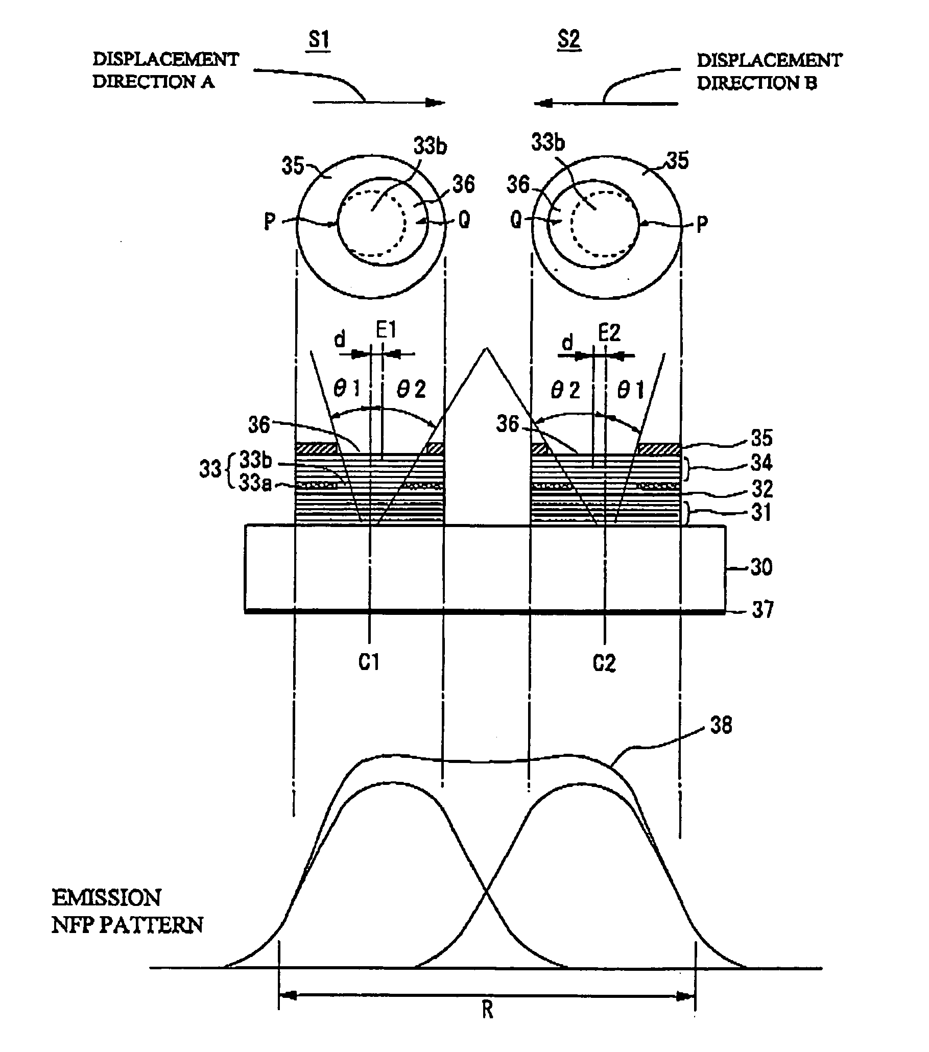
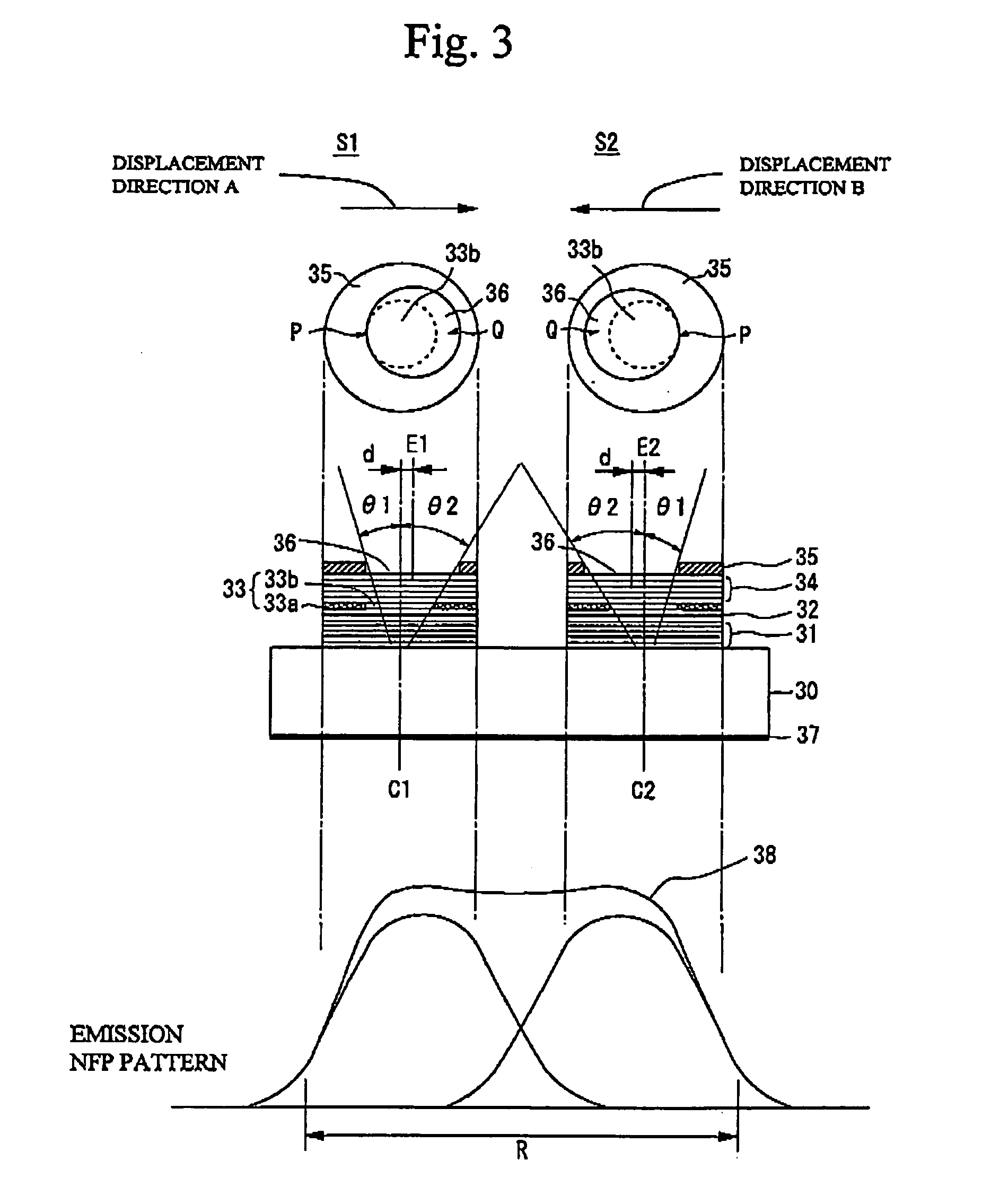
[0052] Multi-spot type VCSELs according to embodiments of the present invention will be described with reference to the accompanying drawings.

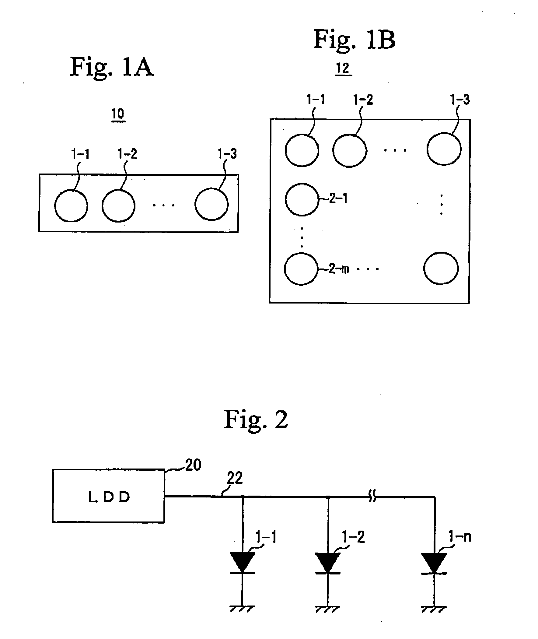
[0053]FIGS. 1A and 1B schematically show plan views of VCSELs according to an embodiment of the present invention. More particularly, FIG. 1A shows a VCSEL array 10 in which light-emitting portions 1-1, 1-2, . . . , 1-n (n is an integer equal to or greater than 2) are arranged so as to form a one-dimensional array. FIG. 1B shows a two-dimensional VCSEL array 12 of m rows and n columns where m and n are integers equal to or greater than 2. The light-emitting portions are formed on a semiconductor substrate, as will be described later, and are simultaneously driven by a drive circuit. The laser beams simultaneously emitted from the light-emitting portions of the array are combined so that laser light with high power can be obtained.

[0054]FIG. 2 shows a circuit diagram of a circuit that drives a VCSEL array of multi-spot type. As shown in FIG. ...


PUM


Abstract

A surface emitting semiconductor laser array includes multiple light-emitting portions arranged in a one-dimensional or two-dimensional array, each of the light-emitting portions including, on a substrate, an active region and a current funneling portion between first and second reflection mirrors, and a light-emission aperture above the second reflection mirror, laser beams being simultaneously emitted from the multiple light-emitting portions. At least one of the multiple light-emitting portions has a near field pattern different from those of other light-emitting portions.

Description

BACKGROUND OF THE INVENTION [0001] 1. Field of the Invention [0002] The present invention relates to a surface emitting semiconductor laser array applicable to light sources of optical interconnections, optical memories, optical switches, optical information processing, laser beam printing machines and copying machines, and an optical transmission system using the array. [0003] 2. Description of the Related Art [0004] A vertical cavity surface emitting laser diode (hereinafter referred to as VCSEL) is an optical device that has a resonator formed in the direction vertical to the semiconductor substrate, and emits light in this vertical direction. Multiple VCSELs are attractive as parallel-arranged optical sources that can be arranged in a one-dimensional or two-dimensional array in highly integrated fashion. [0005] In VCSEL, the carrier and light are confined in the vertical cavity in order to efficiently emit laser light. There are several means for realizing a confinement structur...

Claims


Application Information

Patent Timeline
IPC IPC(8): H01S5/00H01S5/183H01S5/187H01S5/42
CPCH01S5/423H01S5/02212H01S5/02284H01S2301/18H01S5/18394H01S5/4081H01S5/18311H01S5/04254H01S5/04256H01S5/02251
Inventor OMORI, SEIYASAKAMOTO, AKIRAMIYAMOTO, YASUAKIYOSHIKAWA, MASAHIROHANDA, KOHTARO
Owner FUJIFILM BUSINESS INNOVATION CORP
Why Eureka
Try Eureka