High power and high brightness diode-laser array for material processing applications

a diode-laser array, high-power technology, applied in the direction of instruments, semiconductor lasers, polarising elements, etc., can solve the problems of high cost of such power supplies, insufficient power of individual diode-lasers, and complex arrangement of cylindrical and spherical lens elements in the system

Inactive Publication Date: 2009-07-30
COHERENT INC
View PDF37 Cites 56 Cited by
  • Summary
  • Abstract
  • Description
  • Claims
  • Application Information

AI Technical Summary

Problems solved by technology

An individual diode-laser typically does not emit sufficient power for the applications being considered here.
Such a system requires a complicated arrangement of cylindrical and spherical lens elements.
The cost of such power supplies rises in proportion to the deliverable current.
The optical element for rotating the beams, however, is exceedingly complex, as two reflective facets must be provided for each emitter.
Such an element, if made from a thermally stable material, is not suitable for low cost construction or production in commercial volumes.
Further, the arrangement still requires a high-current power supply for the parallel-connected emitters.

Method used


Image

  • High power and high brightness diode-laser array for material processing applications
  • High power and high brightness diode-laser array for material processing applications
  • High power and high brightness diode-laser array for material processing applications

Examples


embodiment 20

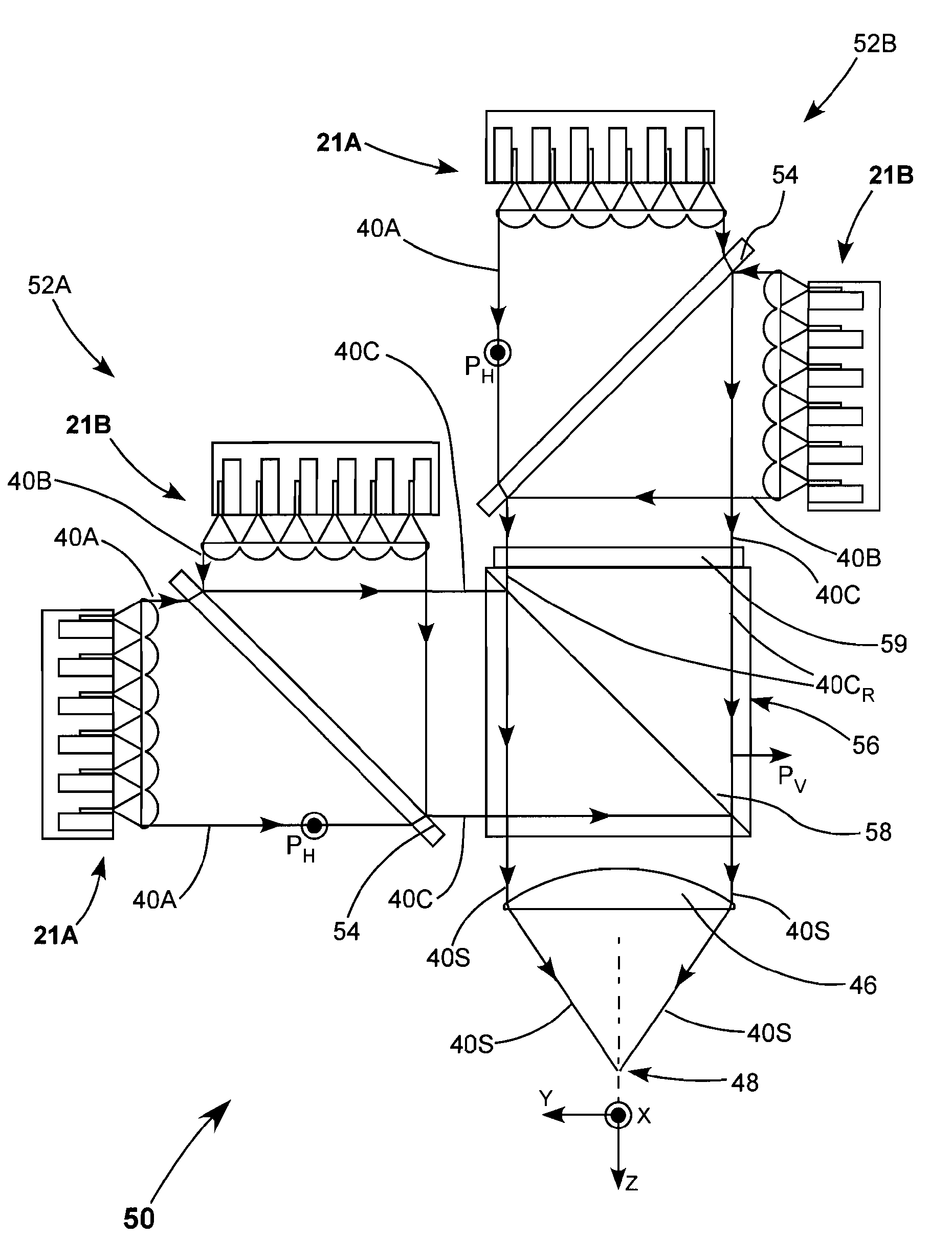
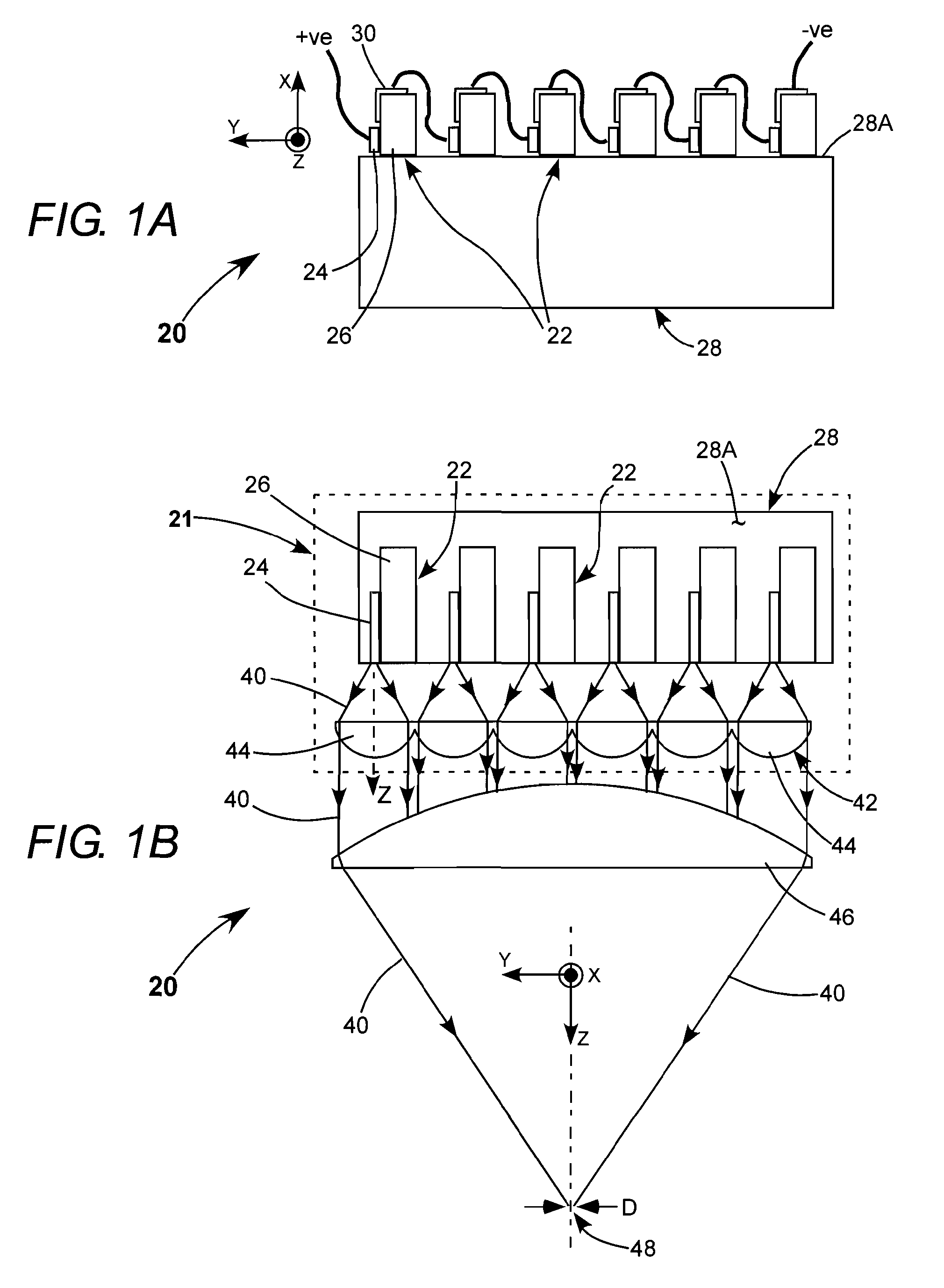
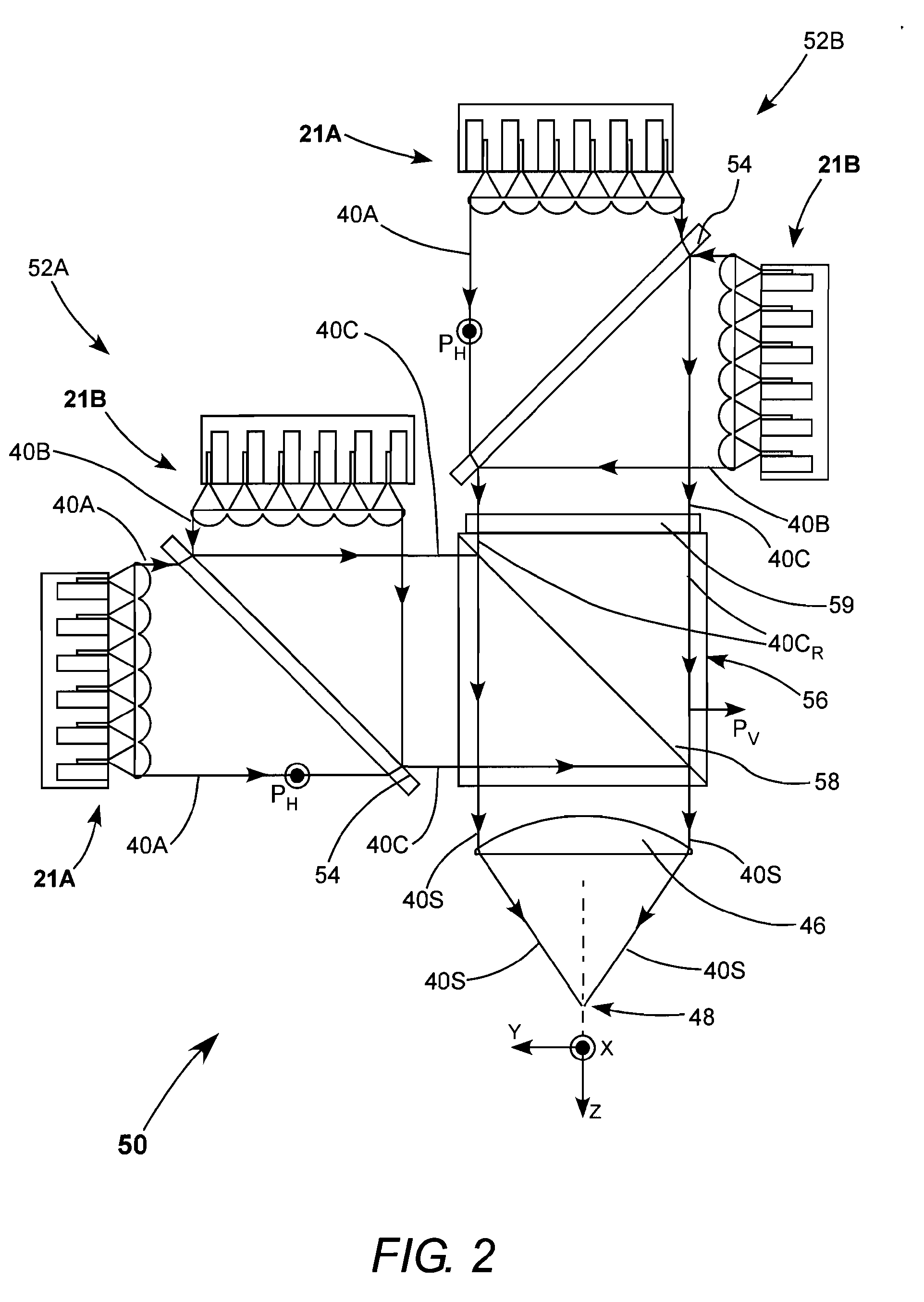
[0025]Referring now to the drawings, wherein like components are designated by like reference numerals, FIG. 1A and FIG. 1B schematically illustrate one preferred embodiment 20 of a diode-laser array package in accordance with the present invention. Package 20 includes a plurality (here, six) of individual diode-laser assemblies 22. Each diode-laser assembly 22 includes a diode-laser 24 mounted on a thermally conductive, electrically insulating submount 26, preferably of diamond, by means of a solder bond. Each submount 26 is bonded to a surface 28A of common heat sink 28. Metallization 30 is provided on each submount to permit electrical contact to the base of the diode-laser. The diode-lasers are electrically connected in series with the upper, strip electrode (not explicitly shown) of one diode-laser being connected to the base of the next as indicated schematically in FIG. 1A.

[0026]As the diode-lasers are depicted in FIG. 1A, each diode-laser would emit a beam perpendicular to t...

embodiment 120

[0051]FIG. 7 is a plan view from above schematically illustrating a further embodiment 120 of a diode-laser array package in accordance with the present invention. FIG. 9 is a three-dimensional view schematically illustrating further details of the package. Package 120 includes eight individual diode-laser packages or sub-assemblies 83, details of which are illustrated in a three-dimensional representation in FIG. 8. Packages 83 as depicted here are DCP™-packages manufactured by Coherent, Inc. of Santa Clara, Calif. Each DCP includes one diode-laser 95 mounted on a heat sink 87. A cylindrical, fast-axis collimating lens 89 is located in front of the diode-laser. Lens 89 is mounted on a spherical ceramic or metal pad 91 which is bonded to heat sink 87. Lens 89 is aligned on pad 91 as described above. A bracket 130 attached to the lens is needed for the tool (such as vacuum chuck) to manipulate the leans during alignment. Electrical contact is made to the diode-laser via tabs 124 (pos...


PUM

PropertyMeasurementUnit
lengthaaaaaaaaaa
lengthaaaaaaaaaa
heightaaaaaaaaaa

Abstract

Arrangements for combination and fast-axis alignment of fast-axes of diode-laser beams are disclosed. Alignment arrangements include providing each diode-laser with a corresponding alignable fast-axis collimating lens, providing individually alignable mirrors for steering an re-orienting beams from each diode-laser, and providing single diode-laser slab-modules in which the diode-laser beams can be pre-aligned to a common propagation-axis direction, and in which edges and surfaces of the slabs can be used to align the fast and slow-axes of the beams. Beam combination methods include combination by dichroic elements, polarization-sensitive elements, and optical fiber bundles.

Description

PRIORITY[0001]This is a divisional application claiming priority to U.S. patent application Ser. No. 11 / 488,578, filed Jul. 18, 2006, which is hereby incorporated herein by reference.TECHNICAL FIELD OF THE INVENTION[0002]The present invention relates in general to arrays of diode-lasers. The invention relates in particular to diode-laser arrays arranged such that either individual diode-lasers or beams from individual diode-lasers are aligned in the fast axis direction of the diode-lasersDISCUSSION OF BACKGROUND ART[0003]Diode-lasers (edge-emitting semiconductor-lasers) provide an efficient source of bright light. Electrical to optical efficiency can be as high as 50%. This high efficiency makes diode-lasers attractive as laser radiation sources for material processing applications and laser welding applications. An individual diode-laser typically has a length between about 1.0 and 1.5 mm. Light is emitted from an aperture that has a height of between about 1.0 micrometers (μm) and...

Claims


Application Information

Patent Timeline
Patent Type & Authority Applications(United States)
IPC IPC(8): G02B27/14H01S3/04G02B27/28G02B27/10G02B27/30
CPCB23K26/0613G02B19/0014G02B27/0994G02B27/283H01S5/005H01S5/0071H01S5/02248H01S5/02252H01S5/02272H01S5/02484H01S5/4012H01S5/4018H01S5/4043H01S5/4056H01S5/4087G02B19/0057G02B19/0028G02B27/0905H01S5/4025H01S5/02326H01S5/0237H01S5/02325
Inventor GOVORKOV, SERGEI V.DIJAILI, SOL PETERANTHON, DOUGLAS WILLIAMSPINELLI, LUIS A.
Owner COHERENT INC
Why Eureka
Try Eureka