Optical scanning device, and image forming apparatus

a scanning device and image forming technology, applied in the field of optical scanning devices and image forming apparatuses, can solve the problems of large scanning line “curve” for a large extent, image quality degradation, and cost and the size of the entire apparatus

Inactive Publication Date: 2008-03-20
RICOH KK
View PDF15 Cites 59 Cited by
  • Summary
  • Abstract
  • Description
  • Claims
  • Application Information

AI Technical Summary

Problems solved by technology

Because the polygon mirror is one of the most expensive optical elements in an optical scanning device, this is an impediment to reducing the cost and the size of the entire apparatus.
However, the oblique-incident optical system has a problem that a scanning line is “curved” for a large extent.
In a monochromatic image forming apparatus, if the scanning lines is curved, image quality degrades.
Furthermore, oblique incidence increases wavefront aberration.
An increase in wavefront aberration leads to degradation of optical performance, especially in image height at the peripheral, and increases a beam-spot diameter, preventing high quality imaging.
However, increased speed causes other problems such as durability of a motor, noise, vibrations, and modulating speed of a semiconductor laser, limiting the recording speed.
There is another problem when a polygon mirror is used as a deflector in an optical scanning device of the oblique-incident optical system with the multi-beam light source that performs multi-beam scanning where a plurality of light beams is written on a single scanned surface simultaneously.
As described above, a multi-beam in the oblique-incident optical system can cause the problems of the sub-scanning beam-pitch variation, due to the light beam shift in the main scanning direction, caused by the sag at the rotating polygon mirror.
In the oblique-incident optical system used for a full-color image forming apparatus, when light beams of different colors to be superimposed differ from each other between the semiconductor lasers 1-1 and 1-2, color shift increasingly occurs in the sub-scanning direction at the peripheral image height, which degrades image quality.

Method used


Image

  • Optical scanning device, and image forming apparatus
  • Optical scanning device, and image forming apparatus
  • Optical scanning device, and image forming apparatus

Examples


first embodiment

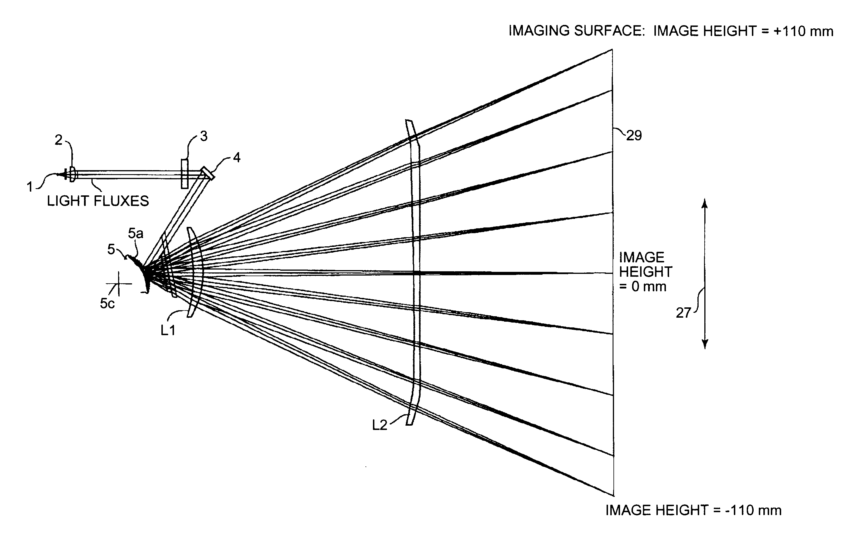
[0045]Exemplary embodiments of the present invention are explained in detail below with reference to the accompanying drawings. Like reference numerals refer to corresponding portions throughout the drawing, and the same explanations are not repeated. Some elements are not shown in the drawings for simplicity of illustration. FIG. 1 is a schematic diagram of an optical scanning device according to the present invention. The optical scanning device includes a semiconductor laser 1 as a light source that emits a light flux (light beams) with divergent quality, and a coupling lens 2 that couples the light flux into a form suited for a subsequent optical system. The light flux can be a parallel one as shown in FIG. 1, or have slight divergent or convergent quality.

[0046]The light flux from the coupling lens 2 is focused on a cylindrical lens 3 in the sub-scanning direction, then folded and reflected on a folding mirror 4 to the reflecting surface of a deflector. The light flux is focuse...

second embodiment

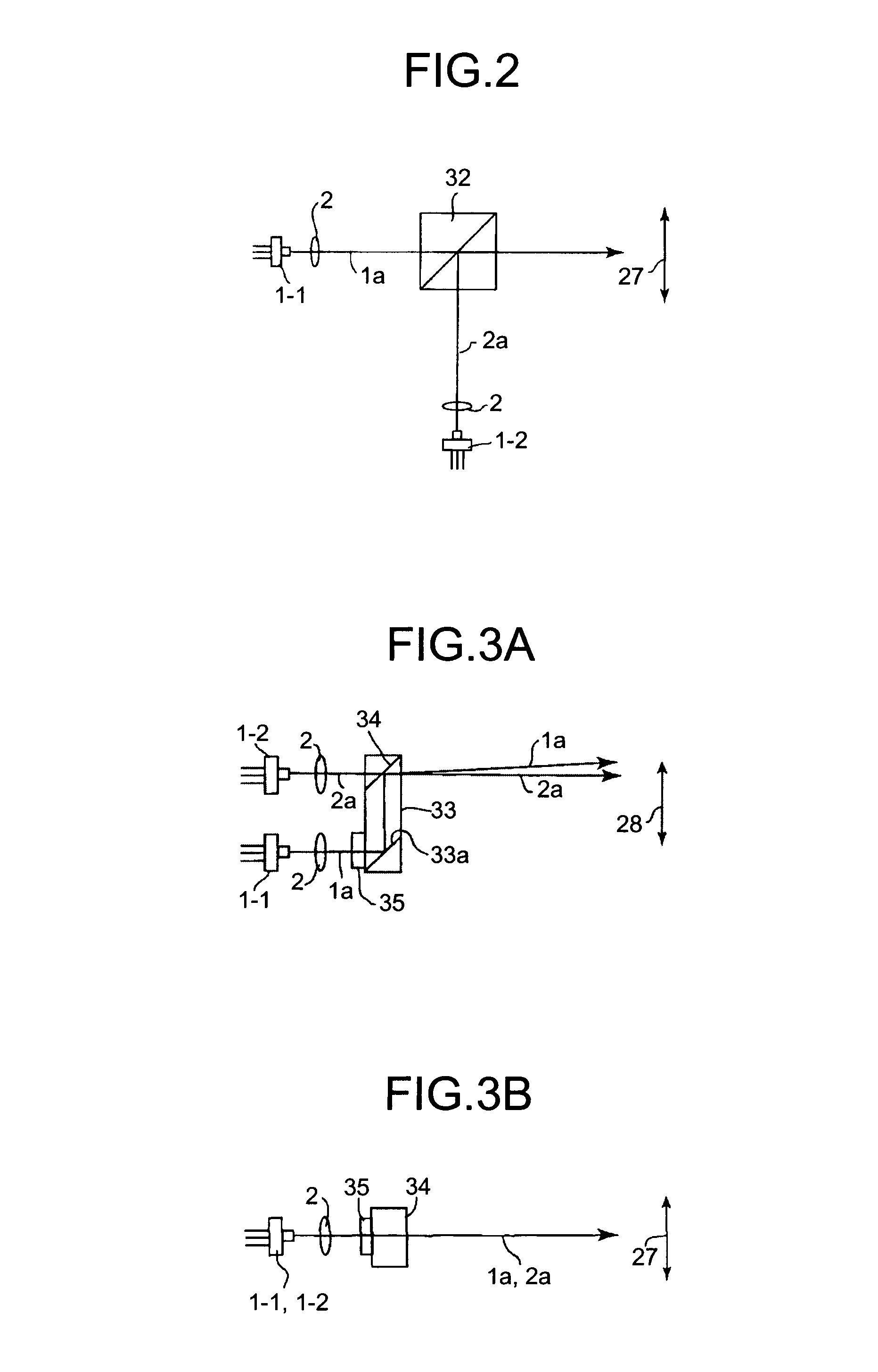
[0059]FIGS. 2, 3A and 3B are schematic diagram of semiconductor lasers 1-1 and 1-2 that emit light beams such that they are incident to the same reflecting surface of the deflector at the same angle with respect to the main scanning direction according to the present invention.

[0060]The first embodiment employs a semiconductor laser array as a light source. An optical scanning device of the second embodiment includes a plurality of the semiconductor lasers 1-1 and 1-2.

[0061]Referring to FIG. 2, one example of the light source structure is explained below. In the second embodiment, a prism 32 is used as a beam-combining unit that brings the light beams closer to each other in the main scanning direction 27. As shown in FIG. 2, the semiconductor lasers 1-1 and 1-2 are arranged separately. Each coupling lens 2 converts each of the light beams 1a and 2a, respectively emitted from the semiconductor lasers 1-1 and 1-2 into a desired form, i.e., for example, parallel, diverging, or converg...

third embodiment

[0068]the present invention relates to an optical scanning device where each of a plurality of light beams that are directed to the same scanned surface cross at the proximity of a reflecting surface, at a different angle with respect to the main scanning direction, upon entering a deflector.

[0069]As an example, a multi-beam-crossing light source is explained. In FIG. 4, the semiconductor lasers 1-1 and 1-2 engage into the engaging holes 405-1 and 405-2, respectively, penetrating through a base member 405. The engaging holes 405-1 and 405-2 are given a slight angle, approximately 1.5° in the third embodiment, with respect to the main scanning direction. Therefore, the semiconductor lasers 1-1 and 1-2, which are engaged into the engaging holes 405-1 and 405-2, are also given the angle of approximately 1.5° with respect to the main scanning direction. The semiconductor lasers 1-1 and 1-2 have a cylinder-shaped heat sink element 1-1a and 1-2a, respectively, on which a cutoff is formed....


PUM


Abstract

An optical scanning device includes a semiconductor laser array is used as the light source, a polygon mirror that has a deflection-reflecting surface and deflects light beams on the deflection-reflecting surface, and a scanning optical system that scans and focuses the light beams on a target surface with a predetermined spacing between the light beams in a sub-scanning direction. The light beams are incident to the deflection-reflecting surface at angles with respect to a normal of the deflection-reflecting surface in the sub-scanning direction, and incident to the deflection-reflecting surface at substantially the same angles in the main scanning direction.

Description

CROSS-REFERENCE TO RELATED APPLICATIONS[0001]The present application claims priority to and incorporates by reference the entire contents of Japanese priority document, 2006-254923 filed in Japan on Sep. 20, 2006.BACKGROUND OF THE INVENTION[0002]1. Field of the Invention[0003]The present invention relates to an optical scanning device, and to an image forming apparatus.[0004]2. Description of the Related Art[0005]Image forming apparatuses such as copiers, facsimile machines, and multifunction products (MFPs) that combine any or all of the functions of copier, facsimile machine, printer, etc. often include an optical scanning device. A typical optical scanning device includes a deflector that deflects light beams from a light source, and a scanning-imaging optical system including an fθ lens that focuses the light beams on a scanned surface to form a light spot thereon. The optical scanning device scans the scanned surface with this light spot (main scanning). The scanned surface ref...

Claims


Application Information

Patent Timeline
Patent Type & Authority Applications(United States)
IPC IPC(8): G02B26/10
CPCG02B26/123
Inventor MIYATAKE, NAOKI
Owner RICOH KK
Why Eureka
Try Eureka