Pattern loading effect reduction for selective epitaxial growth

a technology of epitaxial growth and pattern loading, which is applied in the direction of basic electric elements, electrical equipment, semiconductor devices, etc., can solve the problems of reducing the uniformity of pattern sizes, affecting the development of seg processes, and affecting the uniformity of pattern thickness, so as to reduce the pattern loading effect , the pattern density is more uniform and the pattern loading effect is reduced

Inactive Publication Date: 2006-10-12
TAIWAN SEMICON MFG CO LTD
View PDF4 Cites 57 Cited by
  • Summary
  • Abstract
  • Description
  • Claims
  • Application Information

AI Technical Summary

Benefits of technology

[0007] The preferred embodiment of the present invention provides a method of reducing pattern loading effects for selective epitaxial growth.
[0008] In accordance with one aspect of the present invention, the method includes the steps of forming a mask layer over a substrate, forming an isolation region in the substrate isolating an active region and a dummy active region, removing at least a portion of the mask layer in the active region to form a first opening through which the substrate is exposed, removing at least a portion of the mask layer in the dummy active region to form a second opening through which the substrate...

Problems solved by technology

As a result, the SEG process is different from a general chemical vapor deposition (CVD) process and therefore, unique problems have arisen in the development of the SEG process.
One of the problems is the pattern-loading effect, which occurs due to a difference in pattern density, and which degrades the uniformity of pattern sizes.
Due to a difference in growth rate of a film from one location to another, the amount of growth becomes locally dense or sparse depending on the local pattern density, and this causes a non-uniformity in the thickness o...

Method used


Image

  • Pattern loading effect reduction for selective epitaxial growth
  • Pattern loading effect reduction for selective epitaxial growth
  • Pattern loading effect reduction for selective epitaxial growth

Examples


Embodiment Construction

[0012] The making and using of the presently preferred embodiments are discussed in detail below. It should be appreciated, however, that the present invention provides many applicable inventive concepts that can be embodied in a wide variety of specific contexts. The specific embodiments discussed are merely illustrative of specific ways to make and use the invention, and do not limit the scope of the invention.

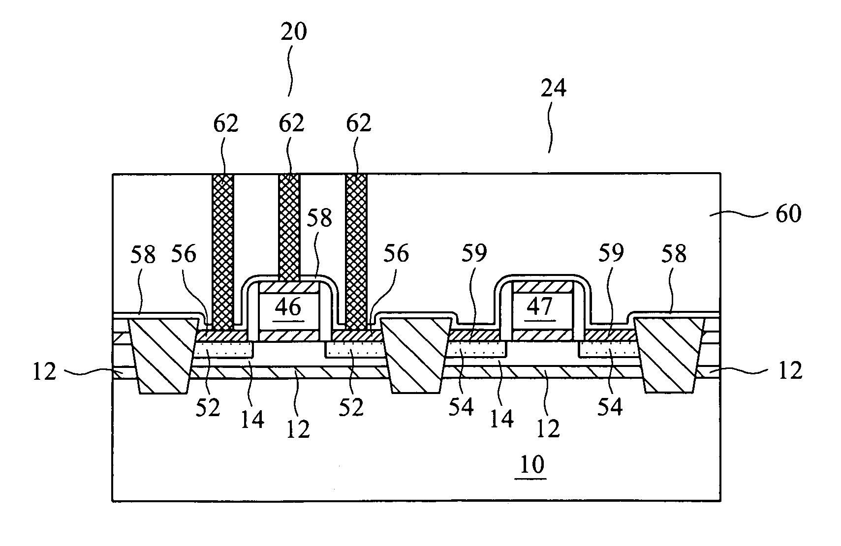
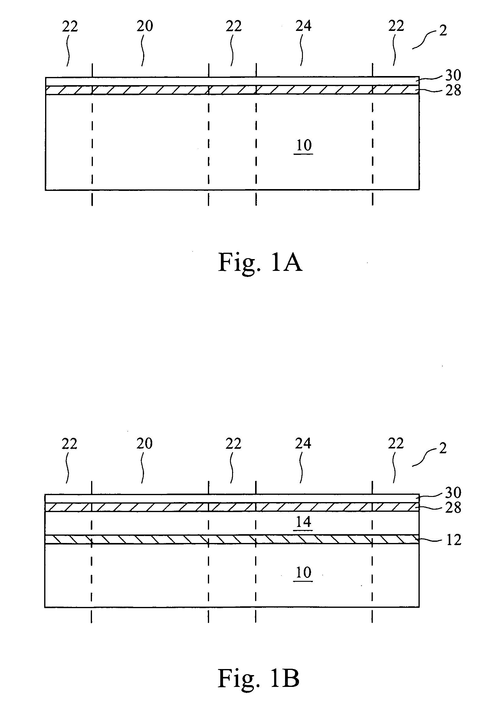
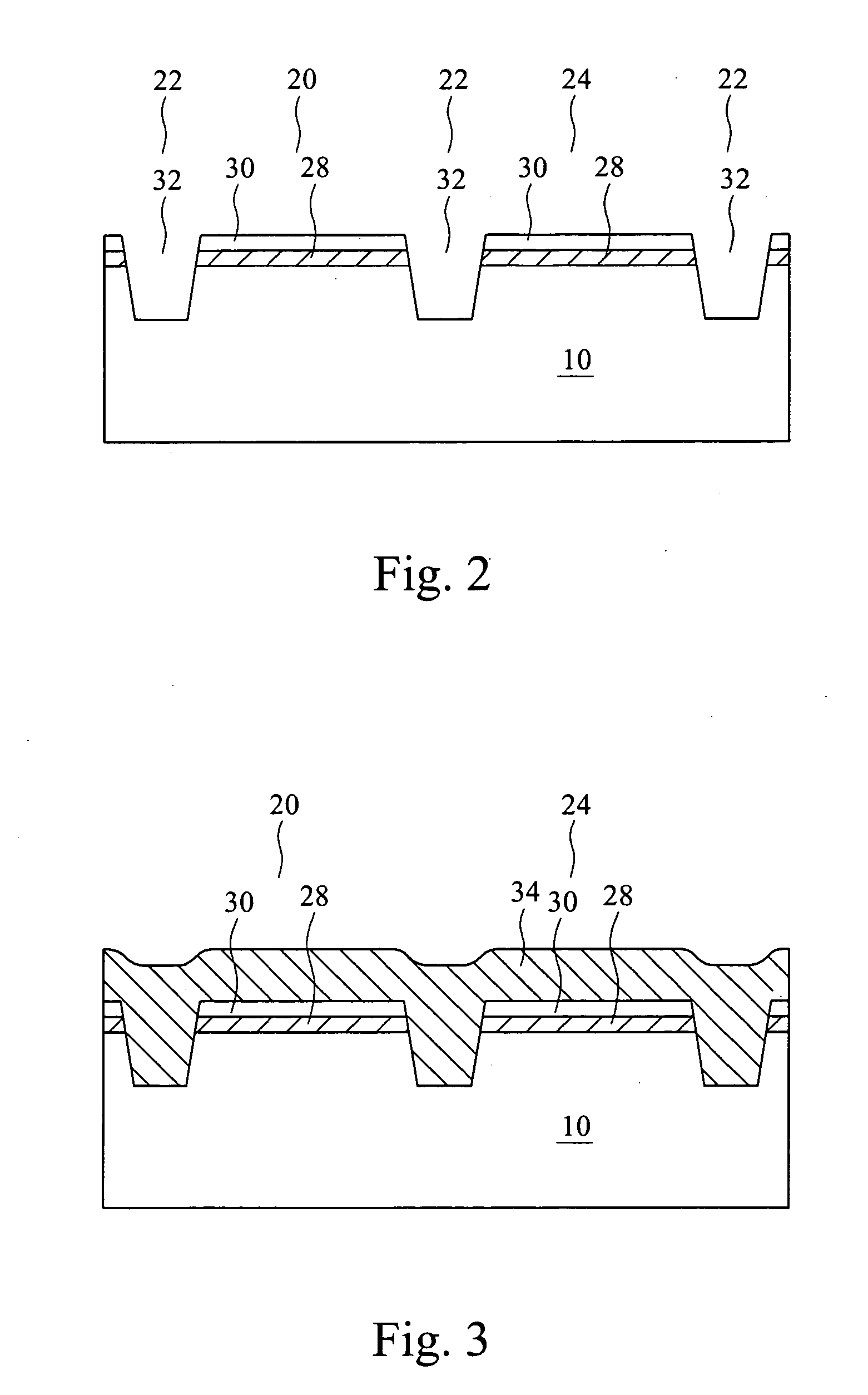
[0013] The cross sectional views of the intermediate stages in the manufacture of preferred embodiments are illustrated in FIGS. 1A through 9B, wherein like reference numbers are used to designate like elements throughout the various views and illustrative embodiments of the present invention. The preferred embodiments of the present invention use the selective growth of source / drain regions as an example. One skilled on the art will realize that the method discussed applies to selective epitaxial growth of other crystal components in integrated circuits as well.

[0014]FIGS...


PUM


Abstract

A method of reducing the pattern-loading effect for selective epitaxial growth. The method includes the steps of: forming a mask layer over a substrate; forming an isolation region in the substrate isolating an active region and a dummy active region; removing at least a portion of the mask layer in the active region and thus forming a first opening, the substrate being exposed through the first opening; removing at least a portion of the mask layer in the dummy active region and thus forming a second opening, the substrate being exposed through the second opening; and performing selective epitaxial growth simultaneously on the substrate in the first opening and second openings. By introducing the second opening wherein epitaxial growth occurs, the pattern density is more uniform and thus the pattern-loading effect is reduced.

Description

TECHNICAL FIELD [0001] This invention relates generally to semiconductor integrated circuits, and more specifically to selective epitaxial processes for semiconductor integrated circuits. BACKGROUND [0002] In order to improve semiconductor integrated device properties, the selective epitaxial growth (SEG) process, also known as selective EPI, was developed. The SEG process has been widely used in strained silicon, elevated source and drain and shallow junction formation. [0003] As is generally known in the art, in the SEG process, single crystal semiconductor material such as silicon or silicon germanium is grown on exposed regions of a semiconductor layer and is not grown on insulating layers such as oxide layers and nitride layers. As a result, the SEG process is different from a general chemical vapor deposition (CVD) process and therefore, unique problems have arisen in the development of the SEG process. One of the problems is the pattern-loading effect, which occurs due to a d...

Claims


Application Information

Patent Timeline
IPC IPC(8): H01L21/8238H01L21/76
CPCH01L21/823807H01L21/823814H01L29/665H01L29/66628H01L29/66636
Inventor TSAI, PANG-YENCHANG, CHIH-CHIENYANG, INDIRALEE, TZE-LIANGCHEN, SHIH-CHANG
Owner TAIWAN SEMICON MFG CO LTD
Why Eureka
Try Eureka