Post-planarization densification

a densification and planarization technology, applied in the field of post-planarization densification, can solve the problems of dielectric material, dielectric material, and structural features of the device having decreased spatial dimensions, and achieve the effect of reducing the pattern loading effect, facilitating densification treatment, and increasing the density of gap-filling silicon oxid

Inactive Publication Date: 2011-04-07
APPLIED MATERIALS INC
View PDF10 Cites 262 Cited by
  • Summary
  • Abstract
  • Description
  • Claims
  • Application Information

AI Technical Summary

Benefits of technology

[0005]Processes for forming high density gap-filling silicon oxide on a patterned substrate are described. The processes increase the density of gap-filling silicon oxide particularly in narrow trenches. The density may also be increased in wide trenches and recessed open areas. The densities of the gap-filling silicon oxide in the narrow and wide trenches / open areas become more similar following the treatment which allows the etch rates to match more closely. This effect may also be described as a reduction in the pattern loading effect. The process involves forming then planarizing silicon oxide. Planarization exposes a new dielectric interface disposed closer to the narrow trenches. The newly exposed interface facilitates a densification treatment by annealing and / or exposing the planarized surface to a plasma.

Problems solved by technology

The decreasing feature sizes result in structural features on the device having decreased spatial dimensions.
The widths of gaps and trenches on the device narrow to a point where the aspect ratio of gap depth to its width becomes high enough to make it challenging to fill the gap with dielectric material.
The depositing dielectric material is prone to clog at the top before the gap completely fills, producing a void or seam in the middle of the gap.
However, once these highly flowable materials are deposited, they may need to be cured and hardened into a solid dielectric material.

Method used


Image

  • Post-planarization densification
  • Post-planarization densification
  • Post-planarization densification

Examples


Embodiment Construction

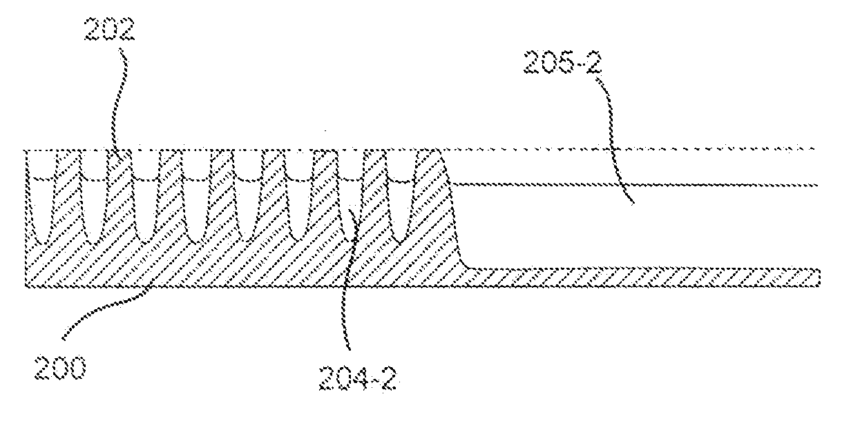
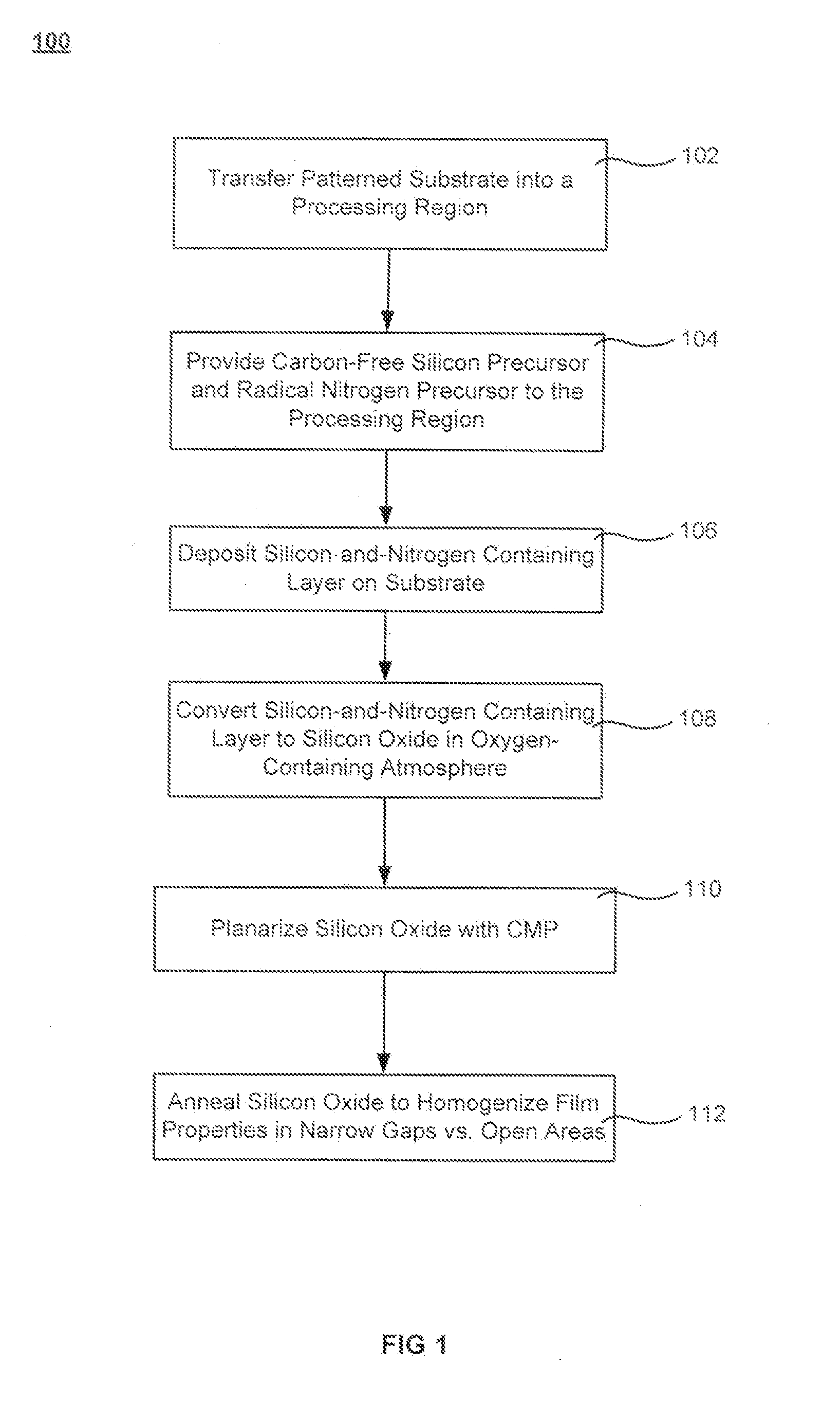
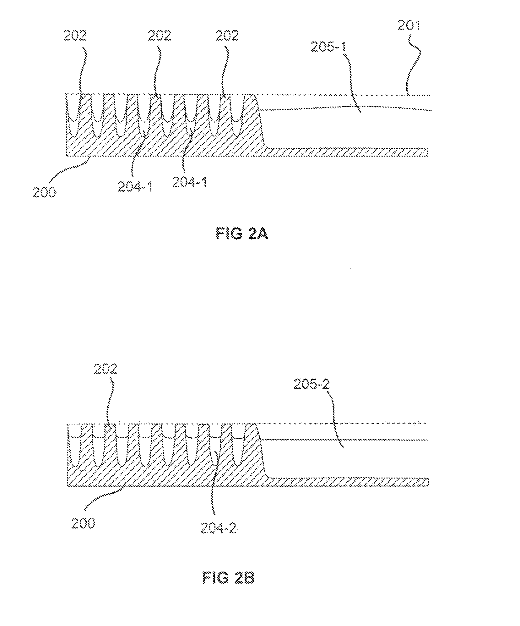
[0015]Processes for forming high density gap-filling silicon oxide on a patterned substrate are described. The processes increase the density of gap-filling silicon oxide particularly in narrow trenches. The density may also be increased in wide trenches and recessed open areas. The densities of the gap-filling silicon oxide in the narrow and wide trenches / open areas become more similar following the treatment which allows the etch rates to match more closely. This effect may also be described as a reduction in the pattern loading effect. The process involves forming then planarizing silicon oxide. Planarization exposes a new dielectric interface disposed closer to the narrow trenches. The newly exposed interface facilitates a densification treatment by annealing and / or exposing the planarized surface to a plasma.

[0016]Dielectric within a trench may possess different properties from dielectric within an open area (or a wide trench). This may result from the more restricted geometry ...


PUM

PropertyMeasurementUnit
widthaaaaaaaaaa
widthaaaaaaaaaa
widthaaaaaaaaaa

Abstract

Processes for forming high density gap-filling silicon oxide on a patterned substrate are described. The processes increase the density of gap-filling silicon oxide particularly in narrow trenches. The density may also be increased in wide trenches and recessed open areas. The densities of the gap-filling silicon oxide in the narrow and wide trenches/open areas become more similar following the treatment which allows the etch rates to match more closely. This effect may also be described as a reduction in the pattern loading effect. The process involves forming then planarizing silicon oxide. Planarization exposes a new dielectric interface disposed closer to the narrow trenches. The newly exposed interface facilitates a densification treatment by annealing and/or exposing the planarized surface to a plasma.

Description

CROSS REFERENCE TO RELATED APPLICATION[0001]This application is a nonprovisional of, and claims the benefit of the filing date of U.S. Provisional Patent Application No. 61 / 248,693, filed Oct. 5, 2009, entitled “POST-PLANARIZATION ANNEAL” by Jingmei Liang et al., the entire disclosure of which is incorporated herein by reference for all purposes.BACKGROUND OF THE INVENTION[0002]Semiconductor device geometries have dramatically decreased in size since their introduction several decades ago. Modern semiconductor fabrication equipment routinely produce devices with 45 nm, 32 nm and 28 nm feature sizes; new equipment is being developed and implemented to make devices with even smaller geometries. The decreasing feature sizes result in structural features on the device having decreased spatial dimensions. The widths of gaps and trenches on the device narrow to a point where the aspect ratio of gap depth to its width becomes high enough to make it challenging to fill the gap with dielectr...

Claims


Application Information

Patent Timeline
Patent Type & Authority Applications(United States)
IPC IPC(8): H01L21/3105
CPCC23C16/345C23C16/452C23C16/56H01L21/02164H01L21/76229H01L21/3105H01L21/31055H01L21/316H01L21/67207H01L21/02337
Inventor LIANG, JINGMEIINGLE, NITIN K.VENKATARAMAN, SHANKAR
Owner APPLIED MATERIALS INC
Why Eureka
Try Eureka