Semiconductor structure and manufacturing method theereof

A manufacturing method and semiconductor technology, applied in semiconductor/solid-state device manufacturing, semiconductor devices, electric solid-state devices, etc., can solve the problems of inconvenience and general products, and achieve the effect of improving pattern uniformity and reducing pattern load effect

Active Publication Date: 2006-06-28
TAIWAN SEMICON MFG CO LTD
View PDF0 Cites 3 Cited by
  • Summary
  • Abstract
  • Description
  • Claims
  • Application Information

AI Technical Summary

Problems solved by technology

[0005] It can be seen that the above-mentioned existing semiconductor structure and its manufacturing method obviously still have inconvenience and defects in structure, method and use, and need to be further improved urgently.
In order to solve the problems existing in the semiconductor structure and its manufacturing method, the relevant manufacturers have tried their best to find a solution, but no suitable design has been developed for a long time, and there is no suitable structure for general products to solve the above problems , this is obviously a problem that relevant industry players are eager to solve

Method used


Image

  • Semiconductor structure and manufacturing method theereof
  • Semiconductor structure and manufacturing method theereof
  • Semiconductor structure and manufacturing method theereof

Examples


Embodiment Construction

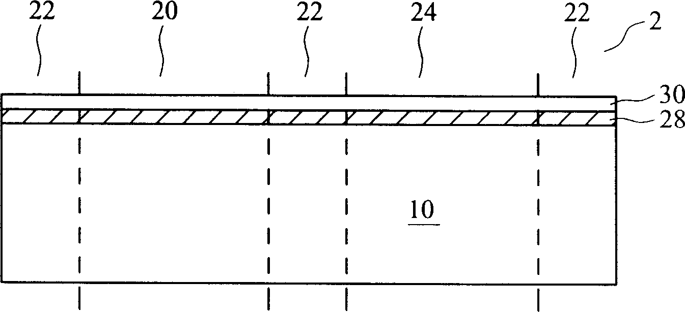
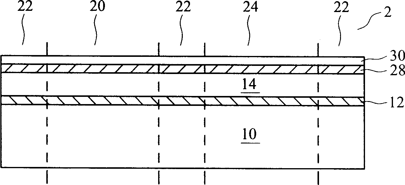
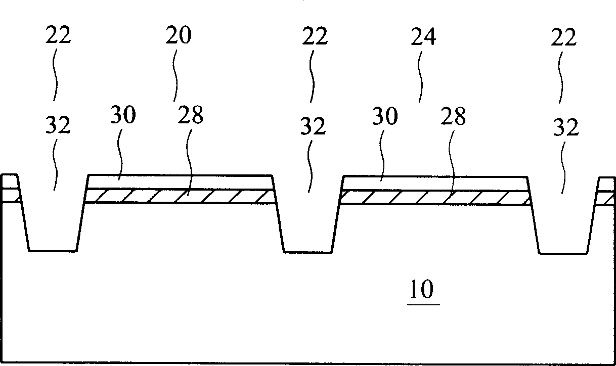
[0043] In order to further explain the technical means and effects that the present invention takes to achieve the intended purpose of the invention, the specific implementation, structure and manufacturing method of the semiconductor structure and its manufacturing method proposed according to the present invention will be described below in conjunction with the accompanying drawings and preferred embodiments. , steps, features and effects thereof are described in detail below.

[0044] see Figure 1A to Figure 9B Shown are cross-sectional views illustrating intermediate stages during fabrication of a preferred embodiment of the invention, wherein like numerals refer to like components throughout the views and illustrated embodiments of the invention. The preferred embodiment of the present invention uses the selective growth of source / drain regions as an example. Those skilled in the art will appreciate that the methods discussed are applicable to the selective epitaxial gr...


PUM


Abstract

The present invention relates to a semiconductor structure and its manufacturing method. The manufacturing method includes the following steps: forming a mask layer on a substrate; forming an isolation region in the substrate to isolate an active region and a dummy active region. area; remove at least a portion of the mask layer in the active area to form a first opening, the first opening exposes the substrate; remove at least a portion of the mask layer in the dummy active area to form a second opening, the second The second opening exposes the substrate; and a selective epitaxial growth step is simultaneously performed on the substrate in the first opening and the second opening. With the introduction of the second opening, the epitaxial growth occurs in the second opening, and the pattern density is more uniform, so the pattern loading effect can be reduced.

Description

technical field [0001] The present invention relates to a semiconductor integrated circuit, and in particular to a semiconductor structure of a selective epitaxy process for the semiconductor integrated circuit and a manufacturing method thereof. Background technique [0002] In order to improve the properties of semiconductor integrated circuit devices, a selective epitaxial growth (SEG) process was developed, also known as selective epitaxial growth. The selective epitaxial growth process has been widely used in the fabrication of strained silicon, elevated source and drain, and shallow junctions. [0003] As is generally known in the art, in a selective epitaxial growth process, a single crystal semiconductor material (such as silicon or silicon germanium) is grown on exposed regions of the semiconductor layer and not on an insulating layer (such as an oxide layer and nitrogen oxide layer). layers). Therefore, the selective epitaxial growth process is different from the...

Claims


Application Information

Patent Timeline
Patent Type & Authority Applications(China)
IPC IPC(8): H01L21/82H01L27/02
CPCH01L21/823807H01L21/823814H01L29/665H01L29/66628H01L29/66636
Inventor 蔡邦彦张志坚杨婷羽李资良陈世昌
Owner TAIWAN SEMICON MFG CO LTD
Why Eureka
Try Eureka