BGA semiconductor chip package and mounting structure thereof

Inactive Publication Date: 2006-10-19
SAMSUNG ELECTRONICS CO LTD
View PDF3 Cites 27 Cited by
  • Summary
  • Abstract
  • Description
  • Claims
  • Application Information

AI Technical Summary

Benefits of technology

[0015] In another embodiment of the present invention, a mounting structure of a BGA semiconductor chip package, the mounting structure includes a BGA semiconductor chip package including, a substrate having first and second surfaces, a semiconductor chip mounted on the first surface of the substrate, and having a plurality of bonding pads on a side not mounted to the substrate, and plurality of in/out (I/O) solder balls and dummy solder balls provided on the second surface of the substrate. The structure further includes a mounting substrate including connection pads and one or more protective layers, wherein the I/O solder balls are connected to the connection pads and the dummy solder balls are connected to the protective layer(s), and wherein a height of the protective layer(s) is higher than a height of the connection pads.
[0016]

Problems solved by technology

In some instances, problems, for example, peeling D of the ball land pads 624 and package cracks B may occur.
These weaknesses may cause problems, for example package cracks A, B solder joint cracks C, and / or peeling D. In the case of a package having a tape wiring substrate chip, during a bending test or handling by an operator, mechanical stresses may generate cracks A, B in areas where solder balls are not formed.
However, the use of the underfill resin 697 may result in an increase in manufacturing cost.
In addition, the underfill resin 697 may make the package more difficult to repair.
The resulting thermal stresses may also cause solder joint cracks.
This may lead to a more complicated manufacturing process.

Method used


Image

  • BGA semiconductor chip package and mounting structure thereof
  • BGA semiconductor chip package and mounting structure thereof
  • BGA semiconductor chip package and mounting structure thereof

Examples


Embodiment Construction

[0031] Example, non-limiting embodiments of the present invention will now be described more fully hereinafter with reference to the accompanying drawings. This invention may, however, be embodied in many different forms and should not be construed as limited to the example embodiments set forth herein. Rather, the disclosed embodiments are provided as working examples. The principles and features of this invention may be employed in varied and numerous embodiments without departing from the scope of the invention.

[0032] Further, well-known structures and processes are not described or illustrated in detail to avoid obscuring the present invention. Like reference numerals are used for like and corresponding parts of the various drawings.

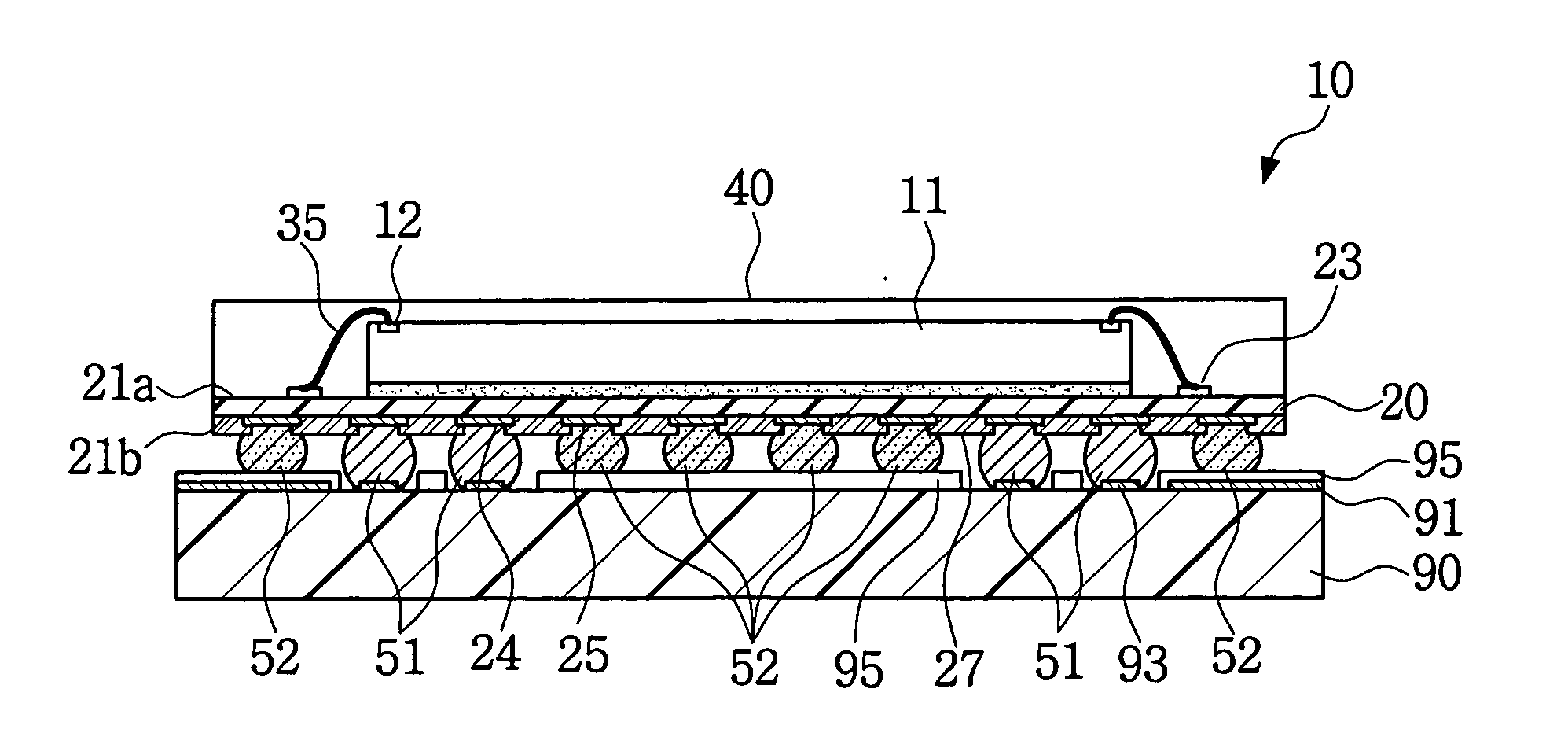
[0033]FIG. 6A is a plan view of a BGA package 10 in accordance with an example embodiment of the present invention. FIG. 6B is a cross-sectional view taken along the line I-I of FIG. 6A.

[0034] Referring to FIGS. 6A and 6B, the BGA package 10 may c...


PUM


Abstract

In example embodiments of the present invention, a structure of a BGA semiconductor chip package includes a substrate having first and second surfaces, a semiconductor chip having a plurality of bonding pads, and mounted on the first surface of the substrate, and plurality of in / out (I / O) solder balls and dummy solder balls provided on the second surface of the substrate, wherein the I / O solder balls are electrically connected to the semiconductor chip and the dummy solder balls are electrically isolated from the semiconductor chip, and the I / O solder balls and the dummy solder balls have the same ball size and ball pitch and are uniformly provided over the second surface of the substrate.

Description

CLAIM OF PRIORITY [0001] A claim of priority under 35 U.S.C. §119 is made to Korean Patent Application No. 2005-32180, filed on Apr. 19, 2005, the entire contents of which are incorporated herein by reference. BACKGROUND OF THE INVENTION [0002] 1. Field of the Invention [0003] Example embodiments of the present invention generally relate to a semiconductor chip package and a mounting structure thereof. More particularly, the present invention relates to a BGA semiconductor chip package and a mounting structure thereof. [0004] 2. Description of the Related Art [0005] A ball grid array (BGA) package may include external connection terminals, for example, solder balls, distributed over a surface of the package. The BGA package was developed in response to increased integration of semiconductor devices and increased number of I / O pins. The BGA package may have a reduced mounting area and / or improved electrical characteristics. [0006] BGA packages may be categorized as a solder mask defi...

Claims


Application Information

Patent Timeline
IPC IPC(8): H01L23/48
CPCH01L23/3128H01L23/49816H01L2224/73265H01L2224/73215H01L2224/32225H01L24/48H05K2201/2036H05K2201/10734H01L23/49838H01L2224/48091H01L2224/48227H01L2224/4824H01L2924/15311H05K3/303H05K3/3436H05K3/3452H05K2201/094H05K2201/09781H01L2924/00014H01L2924/00H01L2924/00012H01L2924/181H01L24/73Y02P70/50H01L2224/45099H01L2224/45015H01L2924/207H02G7/056H02G1/04E04H12/24E04H12/182
Inventor KIM, SANG-YOUNGKIM, JIN-HOPARK, HEE-JINSONG, YOUNG-HEEYOON, TAE-SUNG
Owner SAMSUNG ELECTRONICS CO LTD
Why Eureka
Try Eureka