Nanotubes having controlled characteristics and methods of manufacture thereof

a technology of nanotubes and characteristics, applied in the field of nanotube structures, can solve the problems of limiting the practical production of integrated devices, unable to be effectively handled during the subsequent manufacturing process, and difficult to grow a uniform length nanotube array

Active Publication Date: 2006-10-19
MICRON TECH INC
View PDF25 Cites 69 Cited by
  • Summary
  • Abstract
  • Description
  • Claims
  • Application Information

AI Technical Summary

Problems solved by technology

Though the functional feasibility to integrate nanostructures into micro-devices has been postulated, process couplings and scale mismatches between nano- and micro-fabrication processes limit the practical production of integrated devices.
It has been recognized that growing a uniform length nanotube array would be extremely difficult.
Companies are selling commercial quantities of nanotubes in the form of soot, which cannot be handled effectively during the subsequent manufacturing processes.
None of theses companies have reported commercially viable manufacturing solutions for the mass production of nanotubes.
However, such a method appears relatively limited in scope and applicability.

Method used


Image

  • Nanotubes having controlled characteristics and methods of manufacture thereof
  • Nanotubes having controlled characteristics and methods of manufacture thereof
  • Nanotubes having controlled characteristics and methods of manufacture thereof

Examples


Embodiment Construction

[0026] Generally, the present invention relates to forming nanotubes. In the following detailed description, reference is made to the accompanying drawings hereof, which illustrate specific embodiments in accordance with the present invention. It should be understood that other embodiments may be utilized, and that various structural, process, or structural and process changes may be made to the described embodiments of the present invention without departing from the spirit and scope thereof. In addition, for clarity, like numerals may refer to like elements and functions in the various figures of the drawings and illustrating the different embodiments of the present invention.

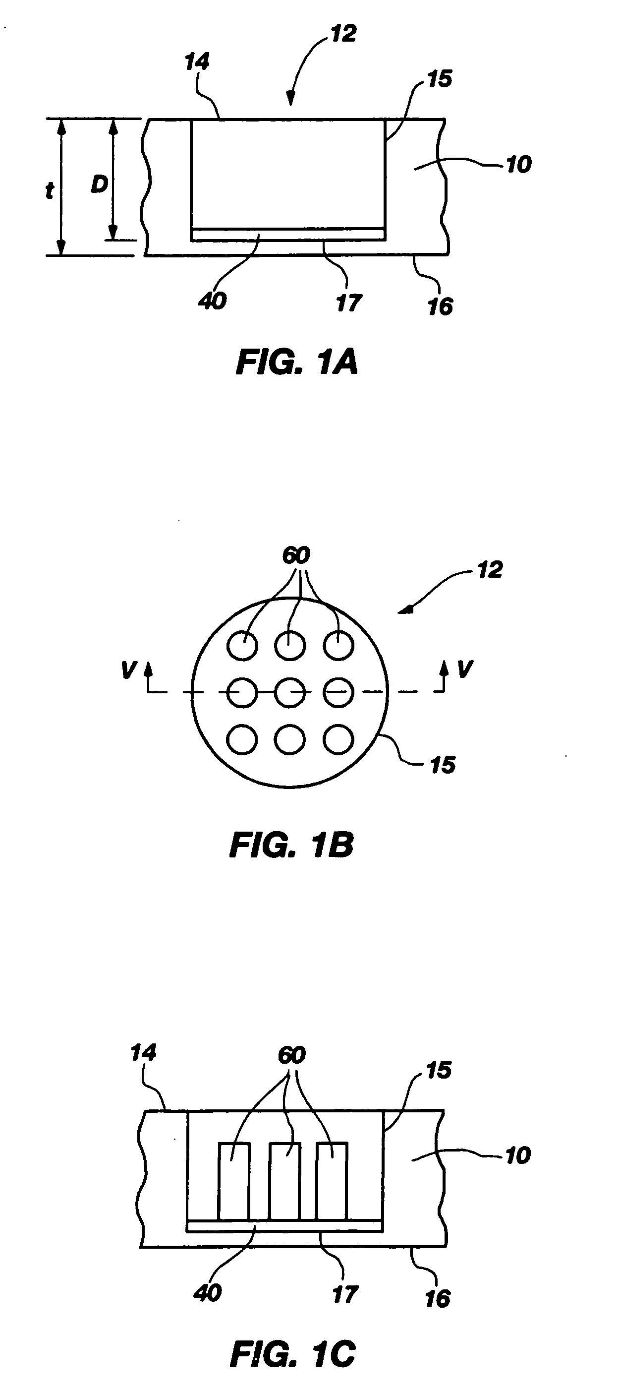
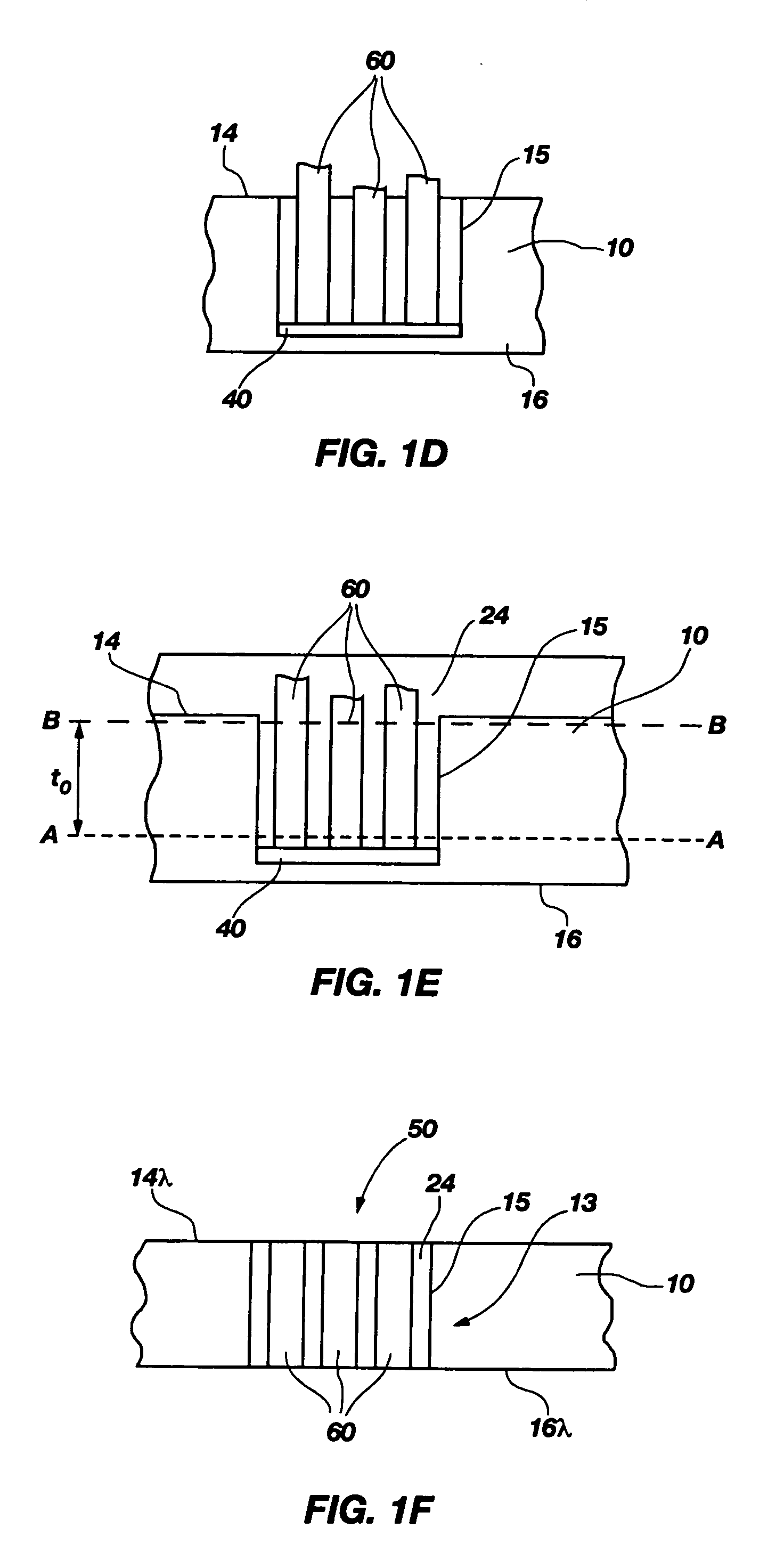
[0027] Exemplary embodiments of methods of manufacture of a plurality of nanotubes according to the present invention will be described with reference to FIGS. 1A-1F, 2A-2C, and 3A-3C.

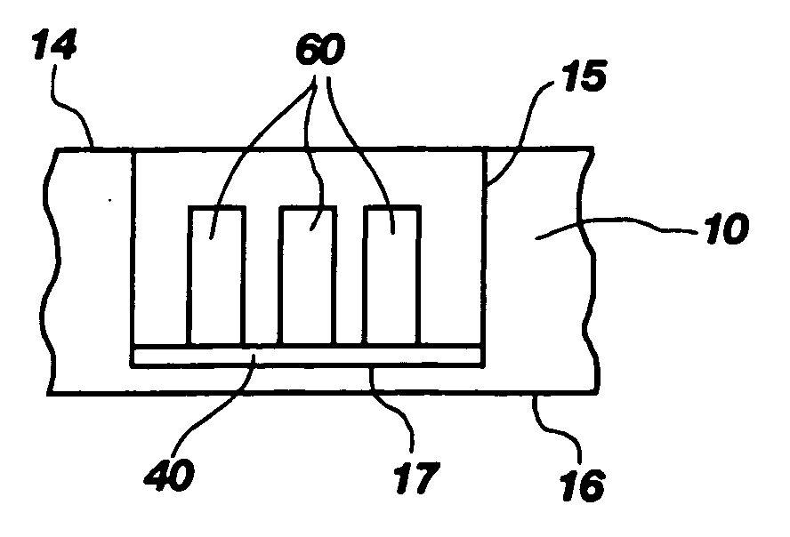
[0028] Referring to FIGS. 1B and 1A, a substrate 10 for forming nanotubes 60 (not shown in FIG. 1A for clarity) is shown in ...


PUM

PropertyMeasurementUnit
diameteraaaaaaaaaa
widthaaaaaaaaaa
diameteraaaaaaaaaa

Abstract

A method of forming a plurality of nanotubes is disclosed. Particularly, a substrate may be provided and a plurality of recesses may be formed therein. Further, a plurality of nanotubes may be formed generally within each of the plurality of recesses and the plurality of nanotubes may be substantially surrounded with a supporting material. Additionally, at least some of the plurality of nanotubes may be selectively shortened and at least a portion of the at least some of the plurality of nanotubes may be functionalized. Methods for forming semiconductor structures intermediate structures, and semiconductor devices are disclosed. An intermediate structure, intermediate semiconductor structure, and a system including nanotube structures are also disclosed.

Description

BACKGROUND OF THE INVENTION [0001] 1. Field of the Invention [0002] The present invention relates to forming a plurality of nanotubes having selective properties, and devices or systems including same. Particularly, the present invention relates to nanotube structures and methods of manufacture thereof. Further, the present invention relates to semiconductor structures and systems including nanotube structures, and methods of manufacture thereof. [0003] 2. Background of Related Art [0004] Several efforts have been made to form nanotubes into patterned configurations (e.g., arrays), however the resulting arrays typically include several nanotubes exhibiting irregular spacing or having varying heights. Other efforts have shown that the growth of aligned nanotubes in several directions can be controlled in a single process. Though the functional feasibility to integrate nanostructures into micro-devices has been postulated, process couplings and scale mismatches between nano- and micro...

Claims


Application Information

Patent Timeline
Patent Type & Authority Applications(United States)
IPC IPC(8): D01F9/12D01C5/00H01L51/40
CPCB82Y10/00D01F9/12H01L51/0048Y10S977/742Y10S977/843Y10S977/862Y10S977/745H01L29/0669H01L21/76897H01L2221/1094Y10S977/842H10K85/221
Inventor SANDHU, GURTEJ S.GILTON, TERRY L.
Owner MICRON TECH INC
Why Eureka
Try Eureka