Multiplexer interface to a nanoscale-crossbar

a multi-layer crossbar and multi-layer technology, applied in the field of multi-layers, can solve the problem that determining the state at a given single-bit storage element by applying a read signal may be significantly more difficul

Active Publication Date: 2006-10-26
HEWLETT-PACKARD ENTERPRISE DEV LP
View PDF5 Cites 15 Cited by
  • Summary
  • Abstract
  • Description
  • Claims
  • Application Information

AI Technical Summary

Benefits of technology

[0009] Various embodiments of the present invention are directed to electronic means for reading the content of a nanowire-crossbar memory. In one embodiment of the present invention, a microscale or submicroscale signal line is interconnected with one set of parallel nanowires emanating from a nanowire-crossbar memory by configurable, nanowire-junction switches. The microscale or submicroscale signal line serves as a single-wire multiplexer, allowing the contents of any particular single-bit storage element within the nanowire-crossbar memory to be read in a three-cycle READ operation.

Problems solved by technology

Significant problems may be encountered with respect to interconnection of individual nanowire leads of a nanowire crossbar to submicroscale and microscale signal lines in order to incorporate the nanowire crossbar into conventional electronic devices, including identifying and manipulating individual nanowires.
By placing a WRITE signal on the nanowires of a nanowire-crossbar memory that intersect at a particular single-bit storage element, the state of the single-bit storage element can be set to a desired one of the two bistable states that encode binary digit values “0” and “1.” However, determining the state at a given single-bit storage element by applying a READ signal may be significantly more difficult.

Method used


Image

  • Multiplexer interface to a nanoscale-crossbar
  • Multiplexer interface to a nanoscale-crossbar
  • Multiplexer interface to a nanoscale-crossbar

Examples


Embodiment Construction

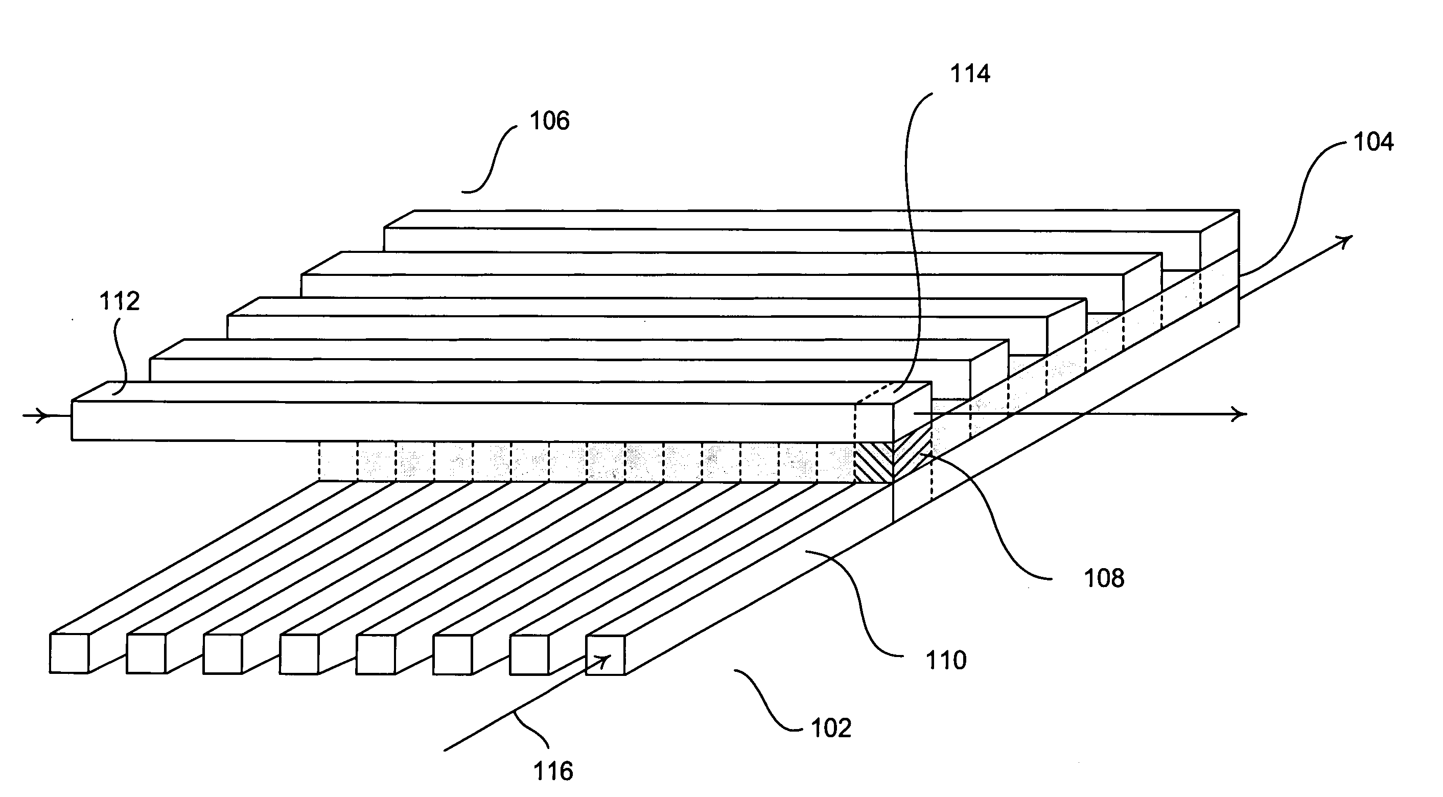
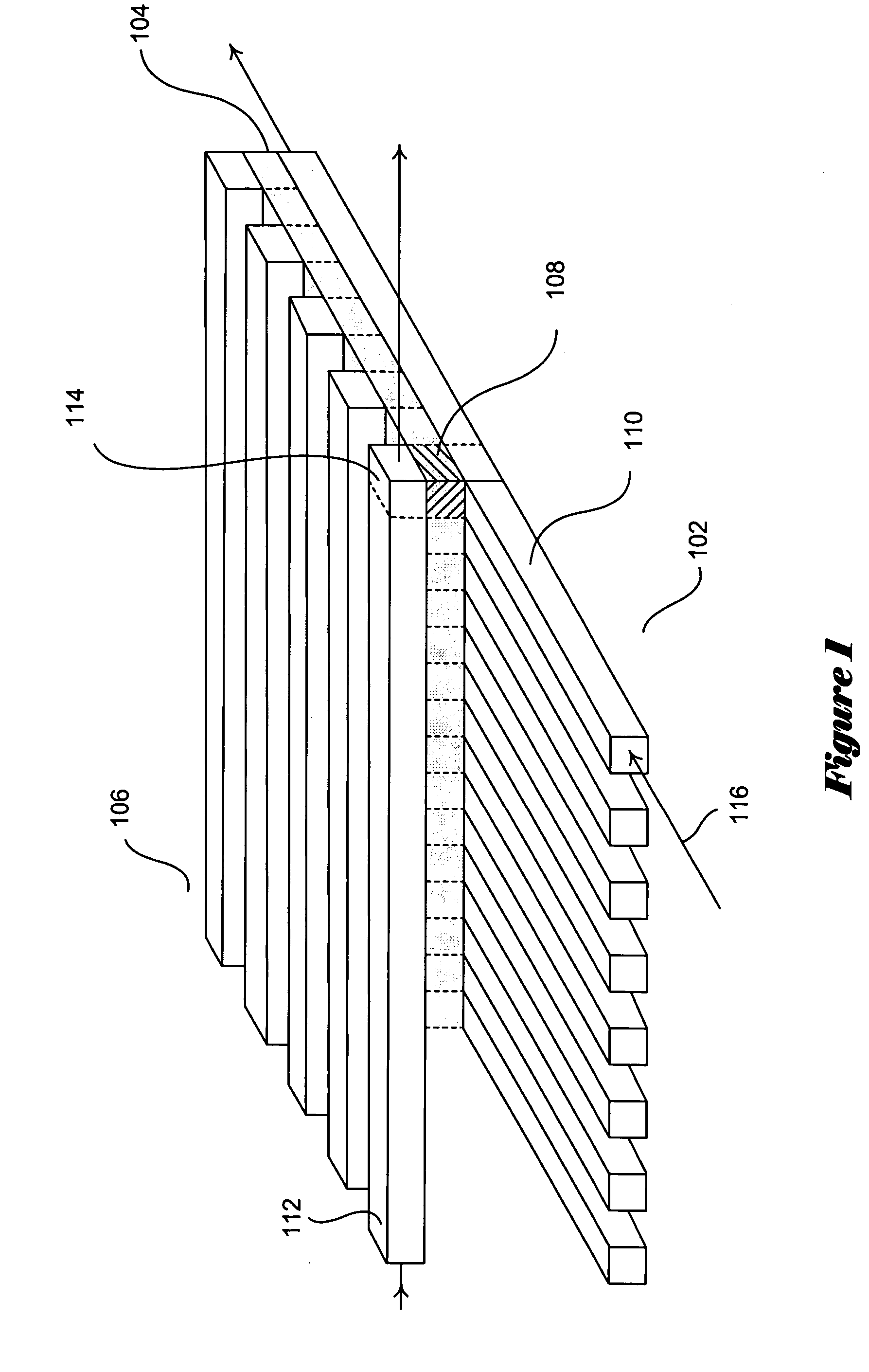
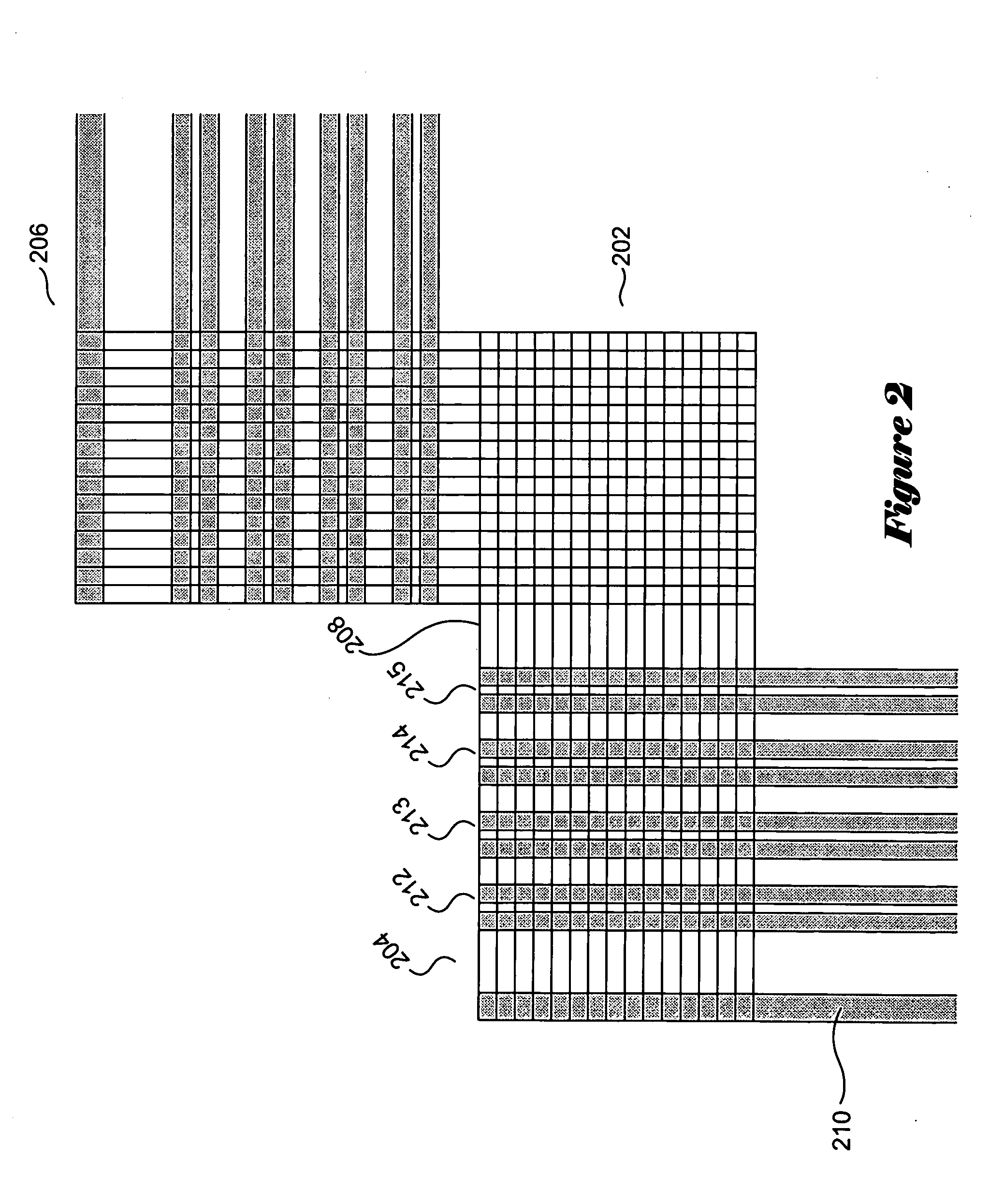
[0014] Various embodiments of the present invention include electronic multiplexers for reading the contents of a selected single-bit storage element within a nanowire-crossbar memory. In the current discussion, the term “nanowire” refers to signal lines with widths less than those of sub-microscale signal lines that can be currently fabricated with conventional photolithographic techniques, less than 50 nanometers, less than 20 nanometers, or less than 10 nanometers. The term nanowire junction refers to an interconnection between a nanowire and another component, whether a second nanowire or a signal line or other component of larger scale. FIGS. 3A-D illustrate a first electronic multiplexer means, a READ operation employing the electronic multiplexer means, and deficiencies and disadvantages of the electronic multiplexer means. FIG. 3A employs illustration conventions used in all of FIGS. 3A-D. In FIG. 3A, a 6×6 nanowire-crossbar memory 302 stores single bits of information at ea...


PUM


Abstract

Various embodiments of the present invention are directed to electronic means for reading the content of a nanowire-crossbar memory. In one embodiment of the present invention, a microscale or sub-microscale signal line is interconnected with one set of parallel nanowires emanating from a nanowire-crossbar memory by configurable, nanowire-junction switches. The microscale or sub-microscale signal line serves as a single-wire multiplexer, allowing the contents of any particular single-bit storage element within the nanowire-crossbar memory to be read in a three-cycle READ operation.

Description

STATEMENT OF GOVERNMENT INTEREST [0001] This invention has been made with Government support under Agreement #MDA972-01-3-005, awarded by DARPA Moletronics. The government has certain rights in the invention.TECHNICAL FIELD [0002] The present invention relates to electronic devices and circuits, and, in particular, to a multiplexer for reading information stored in a nanowire-crossbar memory, and for interfacing a nanowire crossbar to sub-microscale and / or microscale electronics. BACKGROUND OF THE INVENTION [0003] Recently, as the design and manufacture of electronic devices and circuits by conventional, photolithography-based methods has begun to approach physical limits to further decreases in component sizes, alternative methods for manufacturing nanoscale electronic circuits have been developed. Nanowire-crossbar technology is a particularly promising new approach to fabrication of electronic circuits and devices with dimensions significantly less than, and component densities c...

Claims


Application Information

Patent Timeline
Patent Type & Authority Applications(United States)
IPC IPC(8): H01L29/04H03K19/10H01L47/00H03K19/20
CPCB82Y10/00G11C8/10G11C13/0023Y10S977/938G11C2213/77G11C2213/81G11C13/02
Inventor KUEKES, PHILIP J.WILLIAMS, R. STANLEY
Owner HEWLETT-PACKARD ENTERPRISE DEV LP
Why Eureka
Try Eureka