Driving circuit for liquid crystal display device

a technology of driving circuit and liquid crystal display, which is applied in the direction of instruments, static indicating devices, etc., can solve the problems of complicated control process, large layout area, and increase in rc delay, and achieve the effect of simple control structur

Active Publication Date: 2006-10-26
MAGNACHIP SEMICONDUCTOR LTD
View PDF1 Cites 29 Cited by
  • Summary
  • Abstract
  • Description
  • Claims
  • Application Information

AI Technical Summary

Benefits of technology

[0008] Another object of the present invention is to offer a driving circuit for LCD device using a pre-emphasis voltage addition scheme of a more simple control structure.

Problems solved by technology

When an area of LCD is large and its resolution is high, an RC delay increases due to an extended data line of LCD.
However, a structure of the prior art device, as shown in FIG. 4, requires a large layout area and a complicated control process because of six switches therein and support circuits for issuance of signals to control those switches.

Method used


Image

  • Driving circuit for liquid crystal display device
  • Driving circuit for liquid crystal display device
  • Driving circuit for liquid crystal display device

Examples


first embodiment

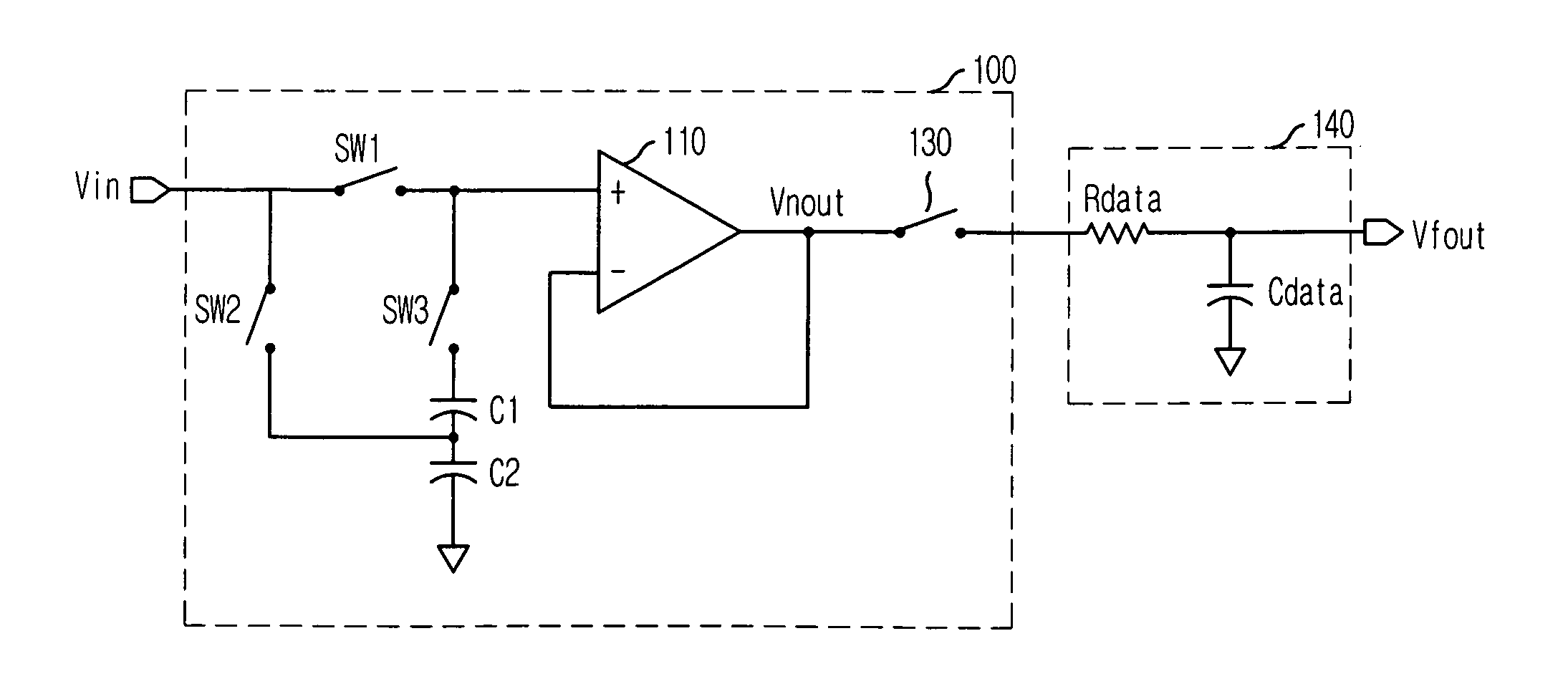
[0025]FIG. 5 illustrates a circuitry diagram of an LCD driving circuit in accordance with the present invention. By employing the LCD driving circuit as shown therein, an image signal voltage amplified under the state that a pre-emphasis voltage is added can be outputted.

[0026] The LCD driving circuit 100 comprises a unity-gain operational amplifier (OP amp) 110 for buffering a signal voltage and carrying it on a transmission line, a first switch SW1 for switching a connection between an input terminal (noninverting terminal) of the unity-gain OP amp 110 and an input line Vin of the signal voltage, a second switch SW2 whose one end is connected to the signal voltage input line Vin, a third switch SW3 whose one end is connected to the input terminal of the unity-gain OP amp 110, a first capacitor C1 whose one end is connected to the other end of the third switch SW3 and other end is connected to the other end of the second switch SW2, and a second capacitor C2 whose one end is connec...

second embodiment

[0036] An LCD driving circuit 200 of the invention, as shown in FIG. 11, comprises a unity-gain OP amp 210 of single gain for buffering a signal voltage and carrying it on a transmission line, a first switch SW11 for switching a connection between an input terminal (noninverting terminal) of the unity-gain OP amp 210 and an input line Vin of the signal voltage, a second switch SW12 whose one end is connected to the signal voltage input line Vin, a third switch SW13 whose one end is connected to the input terminal of the unity-gain OP amp 210, a first capacitor C11 whose one end is connected to the other end of the third switch SW13 and other end is connected to the other end of the second switch SW12, a second capacitor C12 whose one end is connected to the other end of the first capacitor C11 and the other end is connected to the ground voltage terminal, and a fourth switch SW14 arranged between the first and the second capacitors C11 and C12 for switching a connection therebetween...


PUM


Abstract

A driving circuit for Liquid Crystal Display (LCD) device includes a unity-gain operation amplifier (OP amp), three switches, and two capacitors. The unity-gain OP amp buffers and carries a signal voltage on a transmission line. The first switch switches a connection between a noninverting terminal of the unity-gain OP amp and an input line of the signal voltage. One end of the second switch is connected to the input line of the signal voltage. One end of the third switch is connected to the noninverting terminal of the unity-gain OP amp. The first capacitor is connected between the other end of the third switch and the other end of the second switch. The second capacitor is connected between the other end of the first capacitor and the ground voltage terminal.

Description

FIELD OF THE INVENTION [0001] The present invention relates to a driving circuit for Liquid Crystal Display (LCD) device; and, more particularly, to a driving circuit and method adapted to apply to a large-area and high-resolution LCD device. DESCRIPTION OF RELATED ART [0002] An LCD device, one of flat display devices for displaying characters, symbols, or graphics is a display device that combines liquid crystal technology with semiconductor technology using an optical property of liquid crystal that allows molecule array to be varied by an electric field. A Thin Film Transistor-LCD (TFT-LCD) device employs TFT as a switching device that turns on / off its inner pixels, which are turned on / off by turning on / off such TFT. A conventional TFT-LCD device, as shown in FIG. 1, is implemented in such a manner that cells constituting pixels are arranged in an array form, each cell including a liquid crystal cell CLC, a storage capacitor CST, and a TFT serving as a switch. [0003] A source ele...

Claims


Application Information

Patent Timeline
Patent Type & Authority Applications(United States)
IPC IPC(8): G09G3/36
CPCG09G3/3614G09G3/3688G09G2320/0252G09G2310/027G09G2310/0291G09G2310/0248G09G3/20G09G3/36
Inventor LEW, JI-HOSUNG, YOO-CHANGSO, SUN-MAN
Owner MAGNACHIP SEMICONDUCTOR LTD
Why Eureka
Try Eureka