Magnetic memory device

a magnetic memory and memory cell technology, applied in the field of magnetic memory devices, can solve the problems of difficult to further reduce the size of the memory cell and the magnetic memory devi

Active Publication Date: 2006-10-26
TDK CORPARATION
View PDF4 Cites 3 Cited by
  • Summary
  • Abstract
  • Description
  • Claims
  • Application Information

AI Technical Summary

Benefits of technology

[0007] By the way, the inventors have also developed a magnetic memory device including memory cells configured as shown in FIG. 5, based on the above-described conventional magnetic memory device. This magnetic memory device 101 includes only write bit lines 102 formed by a pair of lines 102a and 102b, as write lines, without including the write word line. Further, in the magnetic memory device 101, memory cells 103 are each comprised of a pair of magnetoresistive effect revealing bodies 2a and 2b, a pair of backflow-preventing diodes Da and Db, a pair of transistors (NPN bipolar transistors, for example) TRa and TRb, and an auxiliary write line 104. In this case, the auxiliary write line 104 has opposite ends thereof connected to the lines 102a and 102b, respectively, and is disposed such that a write current flowing through the write bit line 102 is introduced to the vicinity of the magnetoresistive effect revealing bodies 2a and 2b. Further, the transistors TRa and TRb are inserted in the auxiliary write line 104 in a parallel state in which the collector terminal of one of the transistors is connected to the emitter terminal of the other transistor. Further, a data line Dy and a data line Ry are connected to the base terminals of the transistors TRa and TRb. In this case, the same logic information as information to be stored in the memory cell 103 is output to the data line Dy, and logic information opposite to information to be stored in the memory cell 103 is output to the data line Ry.

Problems solved by technology

This complicates the construction of the memory cell 103 itself, thereby making it difficult to further reduce the sizes of the memory cell and the magnetic memory device.

Method used


Image

  • Magnetic memory device
  • Magnetic memory device
  • Magnetic memory device

Examples


Embodiment Construction

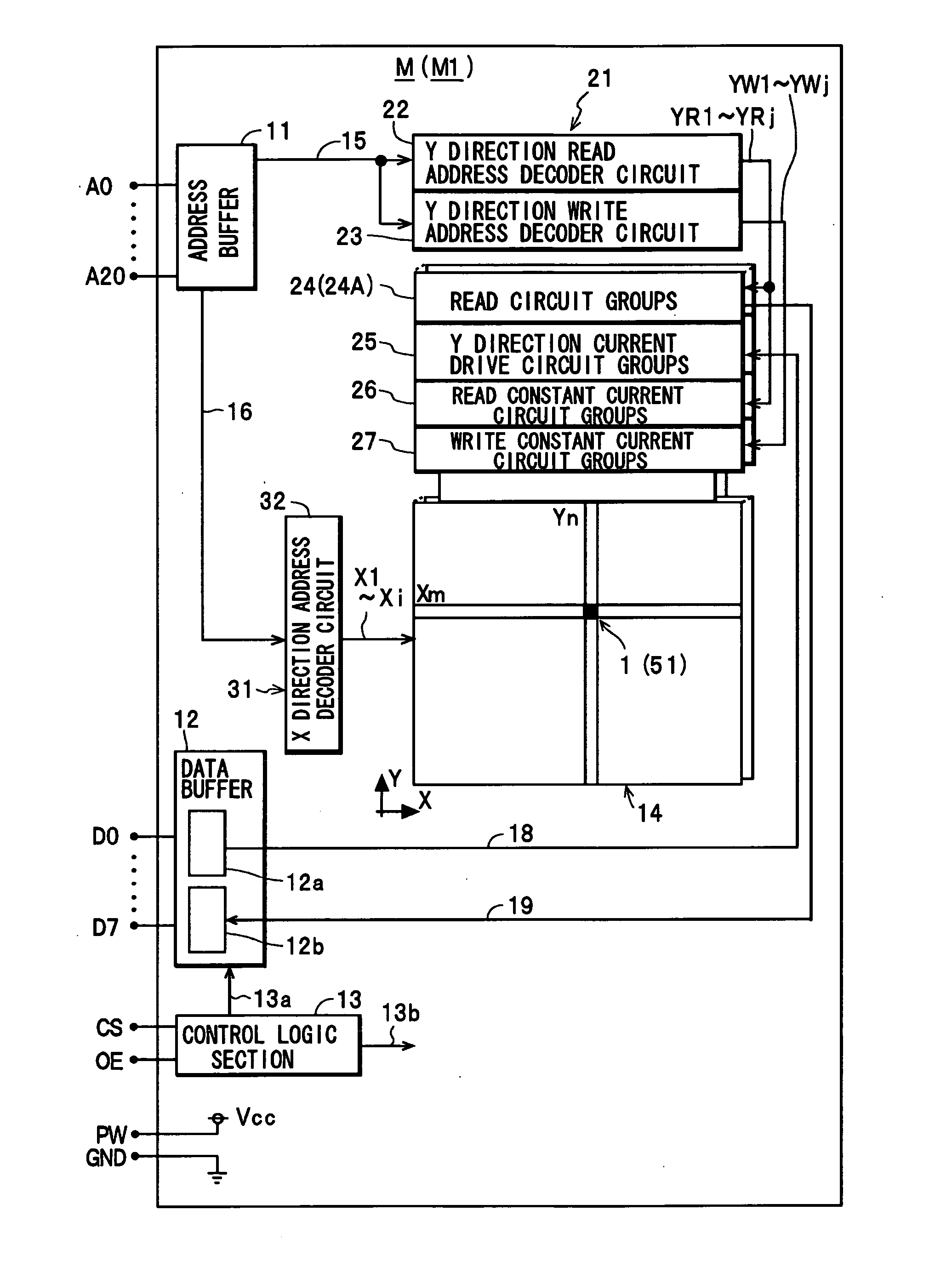
[0026] Hereinafter, an embodiment of the present invention will be described in detail with reference to the drawings.

[0027] First of all, the construction of a magnetic memory device M according to the present embodiment will be described with reference to FIGS. 1 and 2.

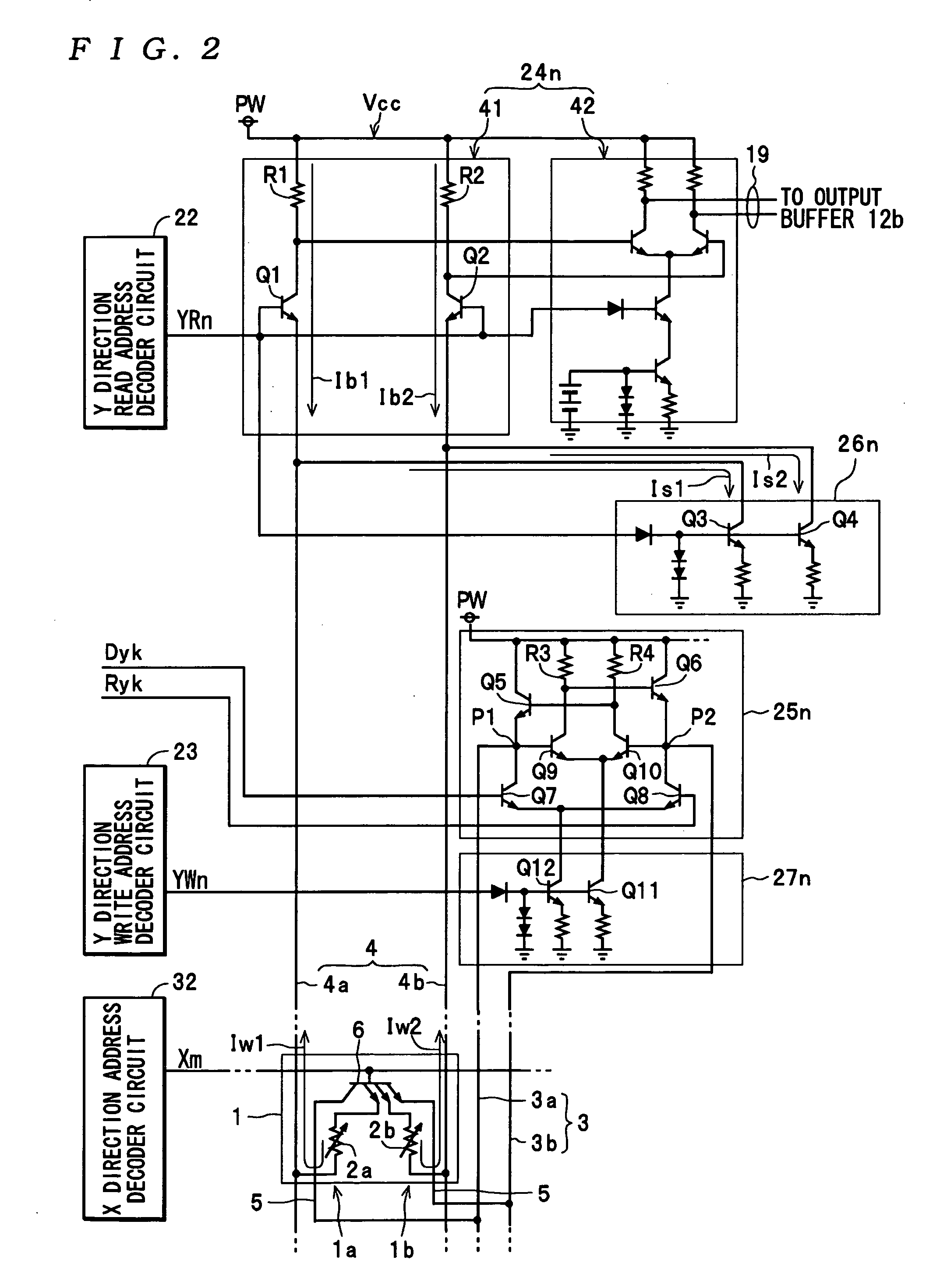
[0028] As shown in FIG. 1, the magnetic memory device M is comprised of an address buffer 11, a data buffer 12, a control logic section 13, memory cell groups 14, a Y direction drive control circuit section 21, and an X direction drive control circuit section 31. In this case, the Y direction drive control circuit section 21 includes a Y direction read address decoder circuit 22, a Y direction write address decoder circuit 23, read circuit groups 24, Y direction current drive circuit groups 25, read constant current circuit groups 26, and write constant current circuit groups 27. On the other hand, the X direction drive control circuit section 31 has an X direction address decoder circuit 32. Further, as to the me...


PUM


Abstract

A magnetic memory device which can be formed with a further reduced size. The magnetic memory device includes: a plurality of memory cells each including at least one magnetoresistive effect revealing body and arranged along a pair of lines; a plurality of auxiliary write lines arranged so that each memory cell is provided with one auxiliary write line, each auxiliary write line being connected to the pair of lines, for introducing write currents flowing through the pair of lines to the vicinity of the magnetoresistive effect revealing body; and transistors arranged so that one transistor is inserted in each auxiliary write line, for allowing the write current to flow bidirectionally through the auxiliary write line in an operating state of the transistors.

Description

BACKGROUND OF THE INVENTION [0001] 1. Field of the Invention [0002] The present invention relates to a magnetic memory device which is provided with memory cells including magnetoresistive effect revealing bodies, and is configured such that information can be recorded thereon and read out therefrom. [0003] 2. Description of the Related Art [0004] As the magnetic memory device of the above-mentioned kind, a magnetic memory device is known which is disclosed in Japanese Laid-Open Patent Publication (Kokai) No. 2004-178623. This magnetic memory device is a magnetic random access memory (hereinafter also referred to as “MRAM”), in which a plurality of memory cells including a pair of magnetoresistive effect revealing bodies (magnetoresistive effect elements) and a pair of backflow-preventing diodes are two-dimensionally arranged. [0005] In the magnetic memory device, an X direction current drive circuit as one write circuit included in an X direction current drive circuit group, and a ...

Claims


Application Information

Patent Timeline
Patent Type & Authority Applications(United States)
IPC IPC(8): G11C11/00
CPCG11C11/16
Inventor EZAKI, JOICHIROKAKINUMA, YUJI
Owner TDK CORPARATION
Why Eureka
Try Eureka