Wafer curvature estimation, monitoring, and compensation

Inactive Publication Date: 2006-10-26
TOKYO ELECTRON LTD
View PDF10 Cites 43 Cited by
  • Summary
  • Abstract
  • Description
  • Claims
  • Application Information

AI Technical Summary

Benefits of technology

[0010] Other embodiments include controlling an actual temperature of each zone using the at least one intelligent set point and thereby establish a substantially uniform critical dimension (CD) profile across the wafer.

Problems solved by technology

When the wafer is treated with heat beyond the acceptable temperature range, a desired photoresist film cannot be obtained.
Because the temperature of the entire hotplate is not uniform and varies with time, it is difficult to determine the temperature of the hotplate by a single temperature sensor at any instant in time.
In addition to the intended results, heat-treating may cause numerous problems.
For example, the light sensitive component of the resist may decompose at temperatures typically used to remove the solvent, which is an extremely serious concern for a chemically amplified resist since the remaining solvent content has a strong impact on the diffusion and amplification rates.

Method used


Image

  • Wafer curvature estimation, monitoring, and compensation
  • Wafer curvature estimation, monitoring, and compensation
  • Wafer curvature estimation, monitoring, and compensation

Examples


Embodiment Construction

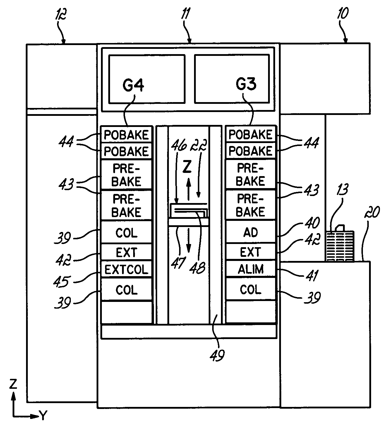
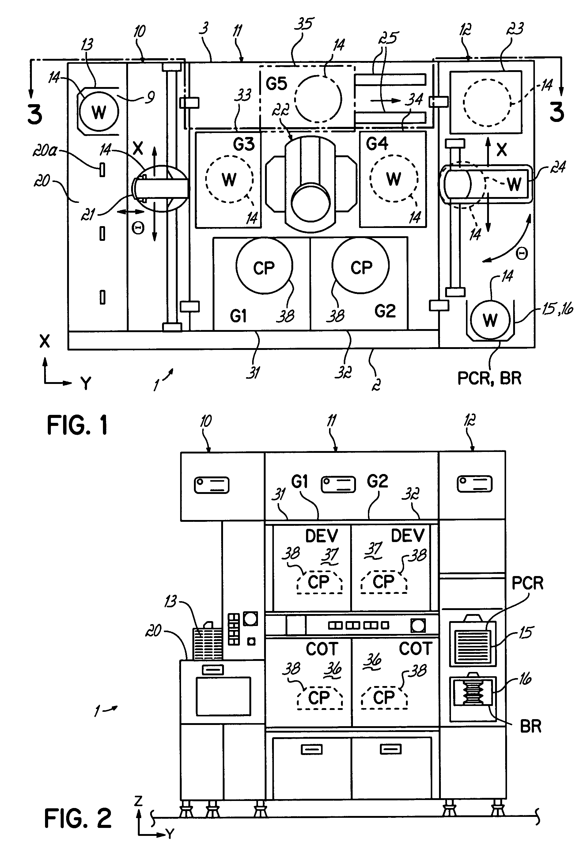
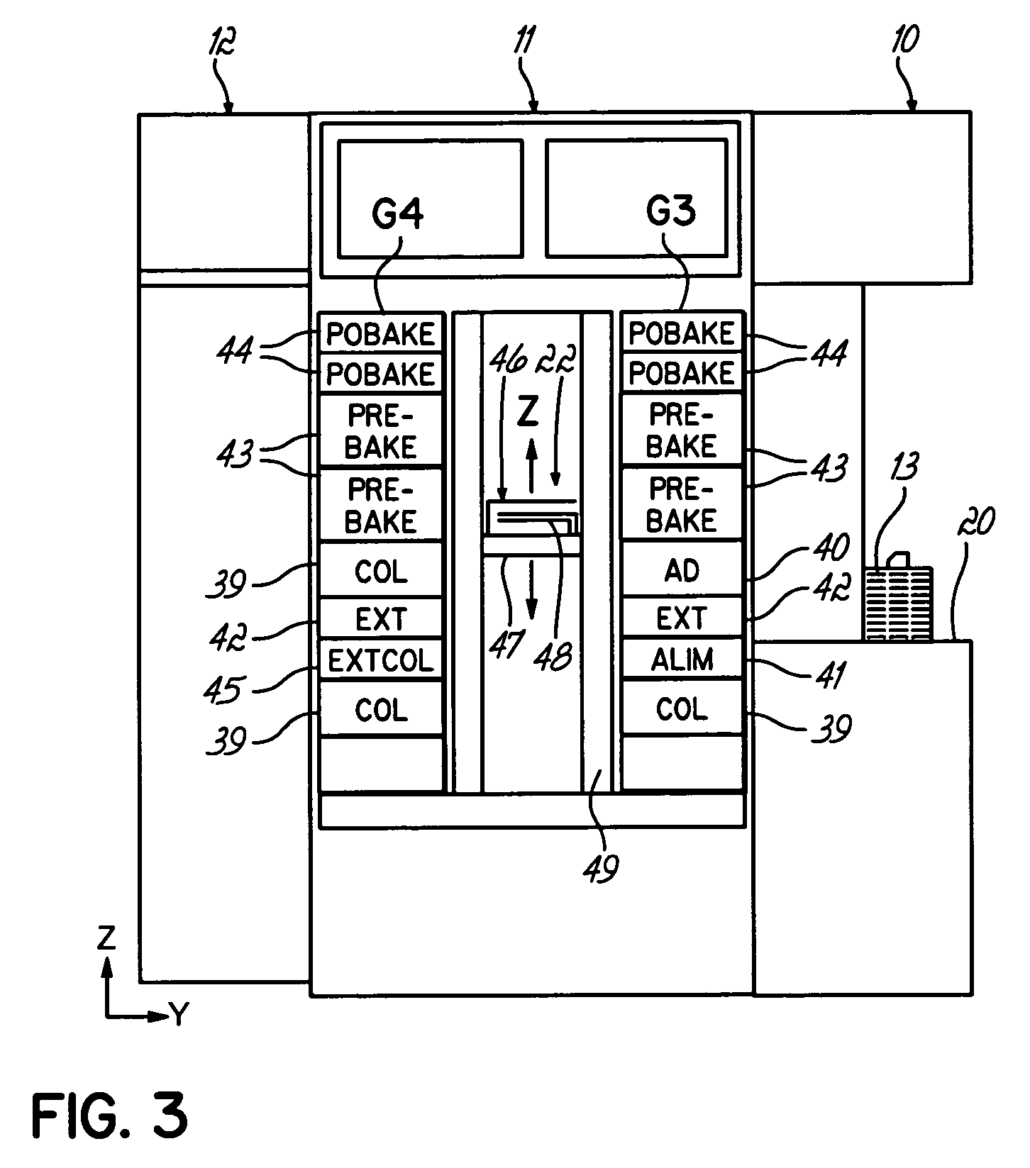
[0032] With reference to FIGS. 1-3, a thermal or coating / developing system 1 has a load / unload section 10, a process section 11, and an interface section 12. The load / unload section 10 has a cassette table 20 on which cassettes (CR) 13, each storing a plurality of semiconductor wafers (W) 14 (e.g., 25), are loaded and unloaded from system 1. The process section 11 has various single wafer processing units for processing wafers 14 sequentially one by one. These processing units are arranged in predetermined positions of multiple stages, for example, within first (G1), second (G2), third (G3), fourth (G4) and fifth (G5) multiple-stage process unit groups 31, 32, 33, 34, 35. The interface section 12 is interposed between the process section 11 and a light-exposure apparatus (not shown).

[0033] A plurality of projections 20a are formed on the cassette table 20. A plurality of cassettes 13 are each oriented relative to the process section 11 by these projections 20a. Each of the cassette...


PUM


Abstract

A method of determining wafer curvature in real-time is presented. The method includes establishing a first temperature profile for a hotplate surface, where the hotplate surface is divided into a plurality of temperature control zones. The method further includes positioning a wafer at a first height above the hotplate surface and determining a second temperature profile for the hotplate surface. The wafer curvature is then determined by using the second temperature profile. Also, a dynamic model of a processing system is presented and wafer curvature can be incorporated into the dynamic model.

Description

CROSS REFERENCE TO RELATED APPLICATIONS [0001] This application is related to co-pending U.S. patent application Ser. No. 10 / 769,623, entitled “Adaptive Real Time Control of a Reticle / Mask System,” Attorney Docket No. TPS-010, filed Jan. 30, 2004, and to U.S. patent application Ser. No.10 / 747,842, entitled “Methods for Adaptive Real Time Control of a Thermal Processing System,” Attorney Docket No. CT-002, filed on Dec. 29, 2003, the contents of which are herein incorporated by reference in their entirety. FIELD OF THE INVENTION [0002] The invention relates to a method for determining the curvature of a substrate, and more particularly, determining the curvature of a semiconductor substrate. BACKGROUND OF THE INVENTION [0003] In a photolithography process for manufacturing semiconductor devices and liquid crystal displays (LCD's), resist is coated on a substrate, and the resultant resist coating film is exposed to light and developed. The series of processing stages are carried out i...

Claims


Application Information

Patent Timeline
IPC IPC(8): G06F15/00
CPCH01L21/67248H01L22/12H01L21/67288
Inventor KAUSHAL, SANJEEVSUGISHIMA, KENJIPANDEY, PRADEEP
Owner TOKYO ELECTRON LTD
Why Eureka
Try Eureka