Piezoelectric oscillation circuit

a technology of oscillation circuit and piezoelectric, applied in the direction of oscillation generator, electrical apparatus, etc., can solve the problems of oscillation circuit stabilization, noise floor deterioration, and difficulty in sufficiently secure a spa

Inactive Publication Date: 2006-11-02
TOYO TSUSHINKI
View PDF8 Cites 26 Cited by
  • Summary
  • Abstract
  • Description
  • Claims
  • Application Information

AI Technical Summary

Benefits of technology

[0019] An advantage of some aspects of the invention is that it provides a piezoelectric oscillation circuit capable of obtaining oscillation characteristic stabilized in a wide power supply voltage range and adjusting the amplitude of an oscillation output.

Problems solved by technology

In this case, it is difficult to sufficiently secure a space for mounting the bypass capacitor Cvreg that is to be inserted in the output line of the stabilized power supply 6.
In addition, since an oscillation output signal becomes easily phase-modulated by the noise generated in the stabilized power supply 6, there is a problem that noise floor of the phase noise characteristic is deteriorated.
In addition, the crystal oscillation circuit stabilizes the reference voltage Vreg while not increasing the operational speed of the stabilized power supply 6 even when the bypass capacitor is not provided.
However, it is difficult to arbitrarily select or adjust the amplitude of the oscillation output voltage by using the configuration of the circuit disclosed in JP-A-2004-255119.

Method used


Image

  • Piezoelectric oscillation circuit
  • Piezoelectric oscillation circuit
  • Piezoelectric oscillation circuit

Examples


Embodiment Construction

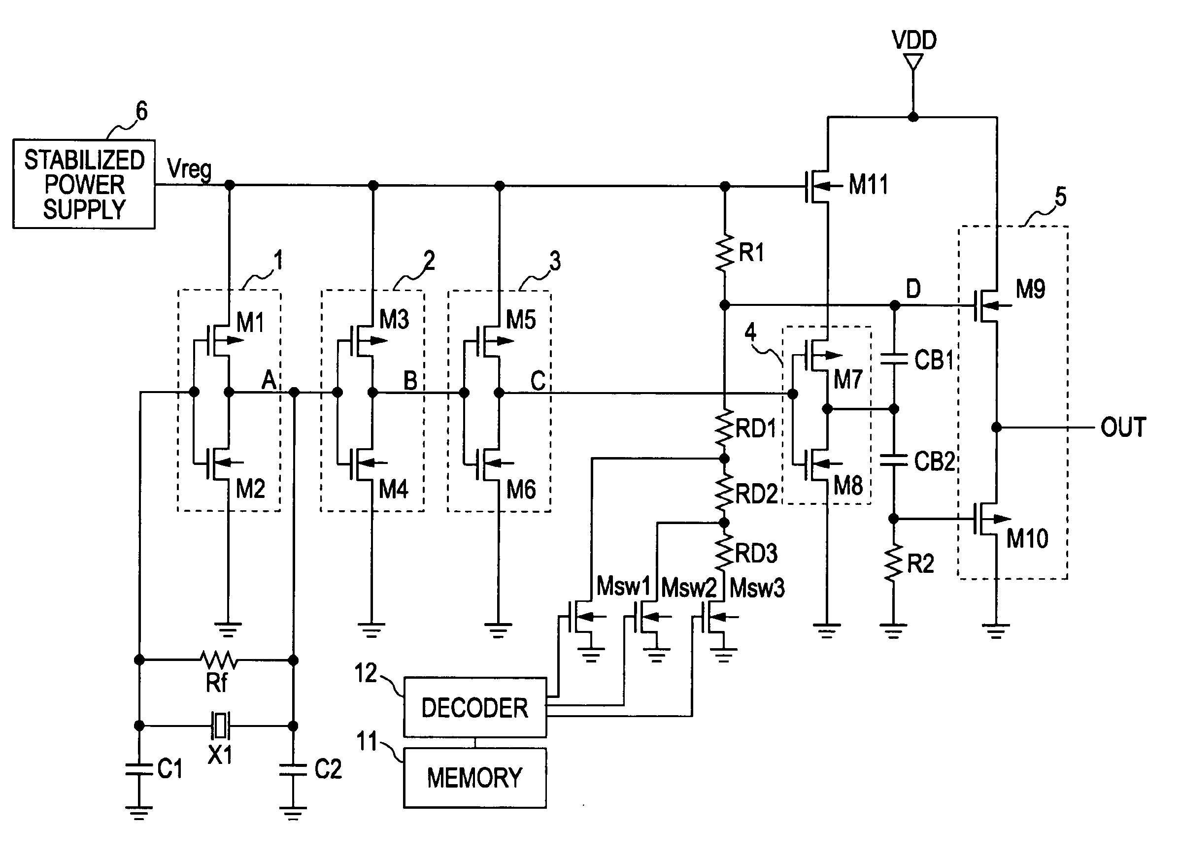
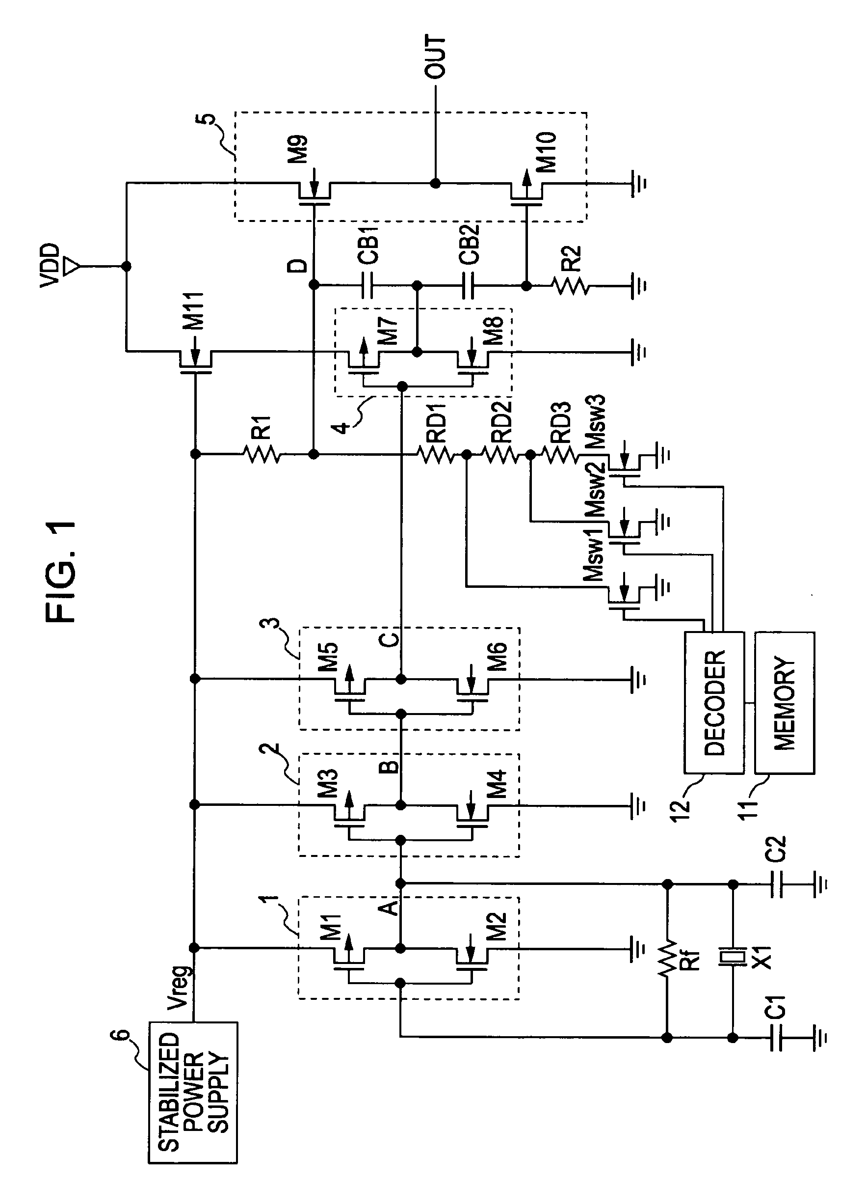
[0035]FIG. 1 is a circuit diagram illustrating a crystal oscillation circuit serving as a piezoelectric oscillation circuit according to an embodiment of the invention.

[0036] In addition, parts of the crystal oscillation circuit having the same functions as in FIGS. 8 and 9 are represented by the same reference numerals, and the descriptions thereof will be omitted.

[0037] In FIG. 1, reference numeral A represents an output terminal of an oscillation amplification circuit 1, reference numeral B represents an output terminal of a first buffer circuit 2, and reference numeral C represents an output terminal of a second buffer circuit 3.

[0038] An output line of a stabilized power supply 6 is connected to a gate of a depletion type MOS transistor M11 and each source of a Pch-CMOS transistor M1 of the oscillation amplification circuit 1, a Pch-CMOS transistor M3 of the first buffer circuit 2, and a Pch-CMOS transistor M5 of the second buffer circuit 3, respectively.

[0039] In addition,...


PUM


Abstract

A piezoelectric oscillation circuit includes: a DC power supply; a stabilized power supply that stabilizes a voltage variation in a DC voltage supplied from the DC power supply; an oscillation circuit unit that uses a piezoelectric vibrator as a vibratory source; a buffer circuit unit to which an output signal output from the oscillation circuit unit is input, a plurality of stages of inverter circuits are connected in series, and a depletion type MOS transistor is connected to the last stage inverter circuit; an output amplification circuit that amplifies an output of the buffer circuit; an output level adjustment circuit that includes a plurality of MOS switches and resistive elements and adjusts an output level by varying a gate voltage of an Nch-transistor included in the output amplification circuit; a memory circuit that stores data for selecting one of the plurality of MOS switches; and a decoder that generates an analog signal to be input to the MOS switch on the basis of the data stored in the memory circuit.

Description

BACKGROUND [0001] 1. Technical Field [0002] The present invention relates to a piezoelectric oscillation circuit, in particular, to a piezoelectric oscillation circuit suitable for use in a low power consumption type temperature compensated crystal oscillator (TCXO). [0003] 2. Related Art [0004] Recently, a mobile device, such as a mobile phone, for mobile communication has been requested to be reduced in size and weight and a crystal oscillation circuit which has been used as a frequency reference of the mobile device has also been requested to be reduced in size. [0005]FIG. 8 is a view illustrating an example of a circuit configuration in a crystal oscillation circuit according to the related art. [0006] In FIG. 8, reference numeral X1 represents a crystal vibrator, reference numeral Rf represents a high-frequency resistor, reference numerals C1 and C2 represent oscillation capacitors, reference numeral 1 represents an oscillation amplification circuit, reference numeral 2 represe...

Claims


Application Information

Patent Timeline
Patent Type & Authority Applications(United States)
IPC IPC(8): H03B5/32
CPCH03B5/04H03B2200/0046H03B2200/0034H03B5/364H03B5/32
Inventor YAMAMOTO, TAKEHIRO
Owner TOYO TSUSHINKI
Why Eureka
Try Eureka