Check patentability & draft patents in minutes with Patsnap Eureka AI!

Semiconductor memory device

Inactive Publication Date: 2006-11-02
KK TOSHIBA
View PDF10 Cites 30 Cited by
  • Summary
  • Abstract
  • Description
  • Claims
  • Application Information

AI Technical Summary

Benefits of technology

[0018] word lines each formed to coupling control gates

Problems solved by technology

In a NAND-type flash memory formed of an SOI substrate, there is a fear of that carriers remained in the NAND cell channel after data write or read operation read to deterioration of the data reliability.
This is such a state that electron injection into an erased cell's floating gate (i.e., electrons thereof have been discharged) easily occurs, and becomes a cause for erratic data write and the like.

Method used


Image

  • Semiconductor memory device
  • Semiconductor memory device
  • Semiconductor memory device

Examples


Embodiment Construction

[0040] Illustrative embodiments of this invention will be explained with reference to the accompanying drawings below.

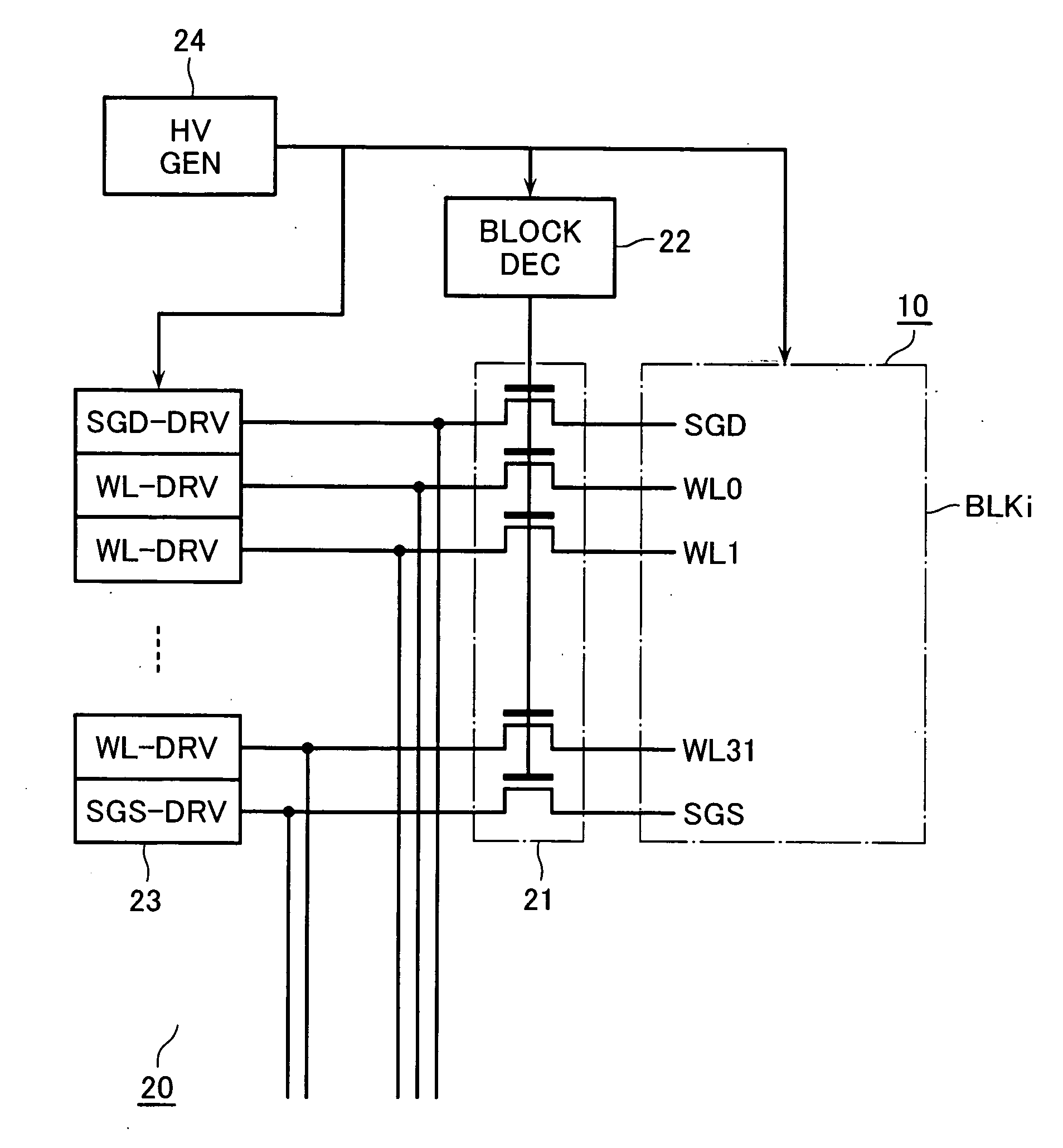
[0041]FIG. 1 is a plan view of a memory cell array 10 in a NAND-type flash memory in accordance with an embodiment of the present invention, and FIGS. 2 and 3 are sectional views thereof taken along lines I-I′ and II-II′, respectively, in FIG. 1.

[0042] The memory cell array 10 is formed on an SOI (Silicon On Insulator) substrate, which has an insulating substrate (i.e., silicon substrate 1 covered with an insulating film 2 such as a silicon dioxide) and a p-type silicon layer 3 formed thereon. The silicon layer 3 is divided into a plurality of active areas (i.e., device forming areas) with a stripe type each, which are separated from each other in the width direction as defined by a device isolation film 4 buried in the silicon layer 3.

[0043] Floating gates 5 are formed on the silicon layer 3 with gate insulating films interposed therebetween; and control gates 6 ...


PUM


Abstract

A semiconductor memory device includes: a semiconductor layer provided on an insulating substrate or an insulating layer; active areas each defined in the semiconductor layer with a device insulating film buried therein; and NAND cell units formed on the active areas, each NAND cell unit including a plurality of electrically rewritable and non-volatile memory cells connected in series, both ends of each NAND cell unit being coupled to a source line and a bit line, wherein the device has such a carrier discharging mode as to discharge channel carriers in the NAND cell unit to at least one of the source line and the bit line.

Description

CROSS-REFERENCE TO RELATED APPLICATION [0001] This application is based on and claims the benefit of priority from the prior Japanese Patent Application No. 2005-133946, filed on May 2, 2005, the entire contents of which are incorporated herein by reference. BACKGROUND OF THE INVENTION [0002] 1. Field of the Invention [0003] This invention relates to a semiconductor memory device with electrically rewritable and non-volatile memory cells, especially to an EEPROM with NAND cell units formed on an SOI substrate. [0004] 2. Description of Related Art [0005] A NAND-type flash memory is known as one of EEPROMs (electrically erasable and programmable ROMs). A NAND-type flash memory is formed of NAND cell units, each of which has a plurality of electrically rewritable and non-volatile memory cells connected in series so that unit cell area thereof is smaller than NOR-type one, and it is easy to achieve a large capacitance. Further, data read and write being performed page by page, a high-sp...

Claims


Application Information

Patent Timeline
IPC IPC(8): G11C16/04
CPCG11C16/0483G11C16/10G11C16/3431
Inventor SHIROTA, RIICHIROARAI, FUMITAKA
Owner KK TOSHIBA
Features
  • R&D
  • Intellectual Property
  • Life Sciences
  • Materials
  • Tech Scout
  • Unparalleled Data Quality
  • Higher Quality Content
  • 60% Fewer Hallucinations
Learn More